SLVU777A September   2012  – November 2021 TPS54020


  1.   Trademarks
  2. 1Introduction
    1. 1.1 Background
    2. 1.2 Performance Specification Summary
    3. 1.3 Modifications
      1. 1.3.1 Output Voltage Setpoint
      2. 1.3.2 Slow-Start Time
      3. 1.3.3 Adjustable UVLO
      4. 1.3.4 Input Voltage Rails
  3. 2Test Setup and Results
    1. 2.1  Input / Output Connections
    2. 2.2  Efficiency
    3. 2.3  Output Voltage Load Regulation
    4. 2.4  Output Voltage Line Regulation
    5. 2.5  Load Transient
    6. 2.6  Control Loop Response
    7. 2.7  Output Voltage Ripple
    8. 2.8  Input Voltage Ripple
    9. 2.9  Start Up
    10. 2.10 Pre-Bias Start Up
    11. 2.11 Hiccup Mode Current Limit
  4. 3Board Layout
    1. 3.1 Layout
  5. 4Schematic and Bill of Materials
    1. 4.1 Schematic
    2. 4.2 Bill of Materials
  6. 5Revision History

Input Voltage Ripple

Figure 2-7 shows the EVM input voltage ripple. The output current is the rated full load of 10 A and VIN = 12 V. The ripple voltage is measured directly across the input capacitors.
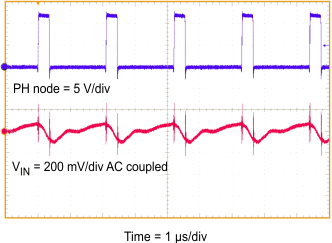
GUID-2E7E9BA5-89D7-446F-8F7C-F5E751393433-low.gif Figure 2-7 TPS54020EVM-082 Input Ripple