SLVU895B March 2013 – January 2022 LMZ31704 , LMZ31707 , LMZ31710
2 Getting Started
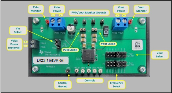
Figure 2-1 highlights the user interface items associated with the EVM. The polarized PVin Power terminal block (TB1) is used for connection to the host input supply and the polarized Vout Power terminal block (TB2) is used for connection to the load. These terminal blocks can accept up to 16-AWG wire. The polarized Vbias terminal block (TB3) is used along with the VIN select jumper (P1) when optional split power supply operation is desired. Refer to the LMZ317xx data sheets (LMZ31710 10-A Module, 2.95-V to 17-V Input and Current Sharing in QFN Package Data Sheet, LMZ31707 7-A Power Module with 2.95-V to 17-V Input Current Sharing in QFN Data Sheet, and LMZ31704 4-A Power Module with 2.95-V to 17-V Input and Current Sharing Data Sheet) for further information on split power supply operation.
 Figure 2-1 LMZ317xxEVM User Interface
The PVin Monitor and Vout Monitor test points located near the power terminal blocks are intended to be used as voltage monitoring points where voltmeters can be connected to measure PVin and Vout. The voltmeter references should be connected to any of the four PVin/Vout Monitor Grounds test points located between the power terminal blocks. Do not use these PVin and Vout monitoring test points as the input supply or output load connection points. The PCB traces connecting to these test points are not designed to support high currents.
The PVin Scope and Vout Scope test points can be used to monitor PVin and Vout waveforms with an oscilloscope. These test points are intended for use with un-hooded scope probes outfitted with a low-inductance ground lead (ground spring) mounted to the scope barrel. The two sockets of each test point are on 0.1 in centers. The scope probe tip should be connected to the socket labeled PVin or Vout, and the scope ground lead should be connected to the socket labeled PGND.
The Controls test points located directly below the device are made available to test the features of the device. Any external connections made to these test points should be referenced to the Control Ground test point located along the bottom of the EVM. Refer to Section 3 for more information on the individual control test points.
The Vout Select jumper (P3) and Fsw Select jumper (P2) are provided for selecting the desired output voltage and appropriate switching frequency. Before applying power to the EVM, ensure that the jumpers are present and properly positioned for the intended output voltage. Refer to Table 2-1 for the recommended jumper settings. Always remove input power before changing the jumper settings.
Once the jumper settings have been confirmed, configure the host input supply to apply the appropriate bus voltage listed in Table 2-1 and confirm that the selected output voltage is obtained.
| VOUT Select | FSW Select | PVin Bus Voltage |
|---|---|---|
| 5.0 V | 1 MHz | 12 V |
| 3.3 V | 750 kHz | 5 V or 12 V |
| 2.5 V | 750 kHz | 5 V or 12 V |
| 1.8 V | 500 kHz | 5 V or 12 V |
| 1.2 V | 300 kHz | 5 V or 12 V |
| 0.9 V | 250 kHz | 5 V or 12 V |
| 0.6 V | 200 kHz | 5 V or 12 V |