SLVUBX2A August 2020 – March 2021 TPS62912 , TPS62913
A Ripple Measurements With Mis-oriented Inductor
This section shows the output ripple measurement results when the inductor is not
installed in its low-noise orientation. This was the case on the Revision A EVMs.


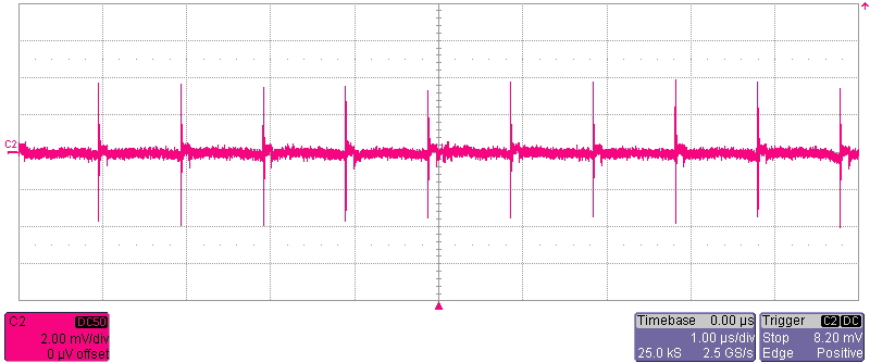
VIN = 12 V,
VOUT = 1.2 V, IOUT = 1000 mA, JP2 Open, Full BW,
DC Coupling, 50-Ω Termination With DC Blocker
Figure A-1 Output Voltage Ripple,
Measured at J4 . 
VIN = 12 V,
VOUT = 1.2 V, IOUT = 1000 mA, JP2 Open, Full BW,
DC Coupling, 50-Ω Termination With DC Blocker
Figure A-2 Output Voltage Ripple,
Measured across C4 With 1x Probe. 
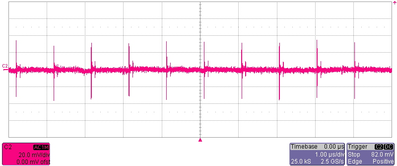
VIN = 12 V,
VOUT = 1.2 V, IOUT = 1000 mA, JP2 Open, Full BW,
AC Coupling, High-Impedance Termination Without DC Blocker
Figure A-3 Output Voltage Ripple,
Measured Across C4 With 10x Probe. 
VIN = 12 V,
VOUT = 1.2 V, IOUT = 1000 mA, JP2 Open, Full BW,
DC Coupling, 50-Ω Termination With DC Blocker
Figure A-4 Output Voltage Ripple,
Measured at J5. 
VIN = 12 V,
VOUT = 1.2 V, IOUT = 1000 mA, JP2 Open, Full BW,
DC Coupling, 50-Ω Termination With DC Blocker
Figure A-5 Output Voltage Ripple,
Measured Across C7 With 1x Probe. 
VIN = 12 V,
VOUT = 1.2 V, IOUT = 1000 mA, JP2 Open, Full BW,
AC Coupling, High-impedance Termination Without DC Blocker
Figure A-6 Output Voltage Ripple,
Measured Across C7 With 10x Probe.