SLVUC34 March   2021 TPS2521


  1.   Trademarks
  2. 1Introduction
    1. 1.1 EVM Features
    2. 1.2 EVM Applications
  3. 2Description
  4. 3Schematic
  5. 4General Configurations
    1. 4.1 Physical Access
    2. 4.2 Test Equipment and Set up
      1. 4.2.1 POWER SUPPLIES
      2. 4.2.2 METERS
      3. 4.2.3 OSCILLOSCOPE
      4. 4.2.4 LOADS
  6. 5Test Setup and Procedures
    1. 5.1 Start up the eFuse
    2. 5.2 Over Current Test
    3. 5.3 Output Hot-Short Test
    4. 5.4 Power Up into Short Test
    5. 5.5 Overvoltage Clamp Test
    6. 5.6 Reverse Current Blocking Test
  7. 6EVAL Board Assembly Drawings and Layout Guidelines
    1. 6.1 PCB Drawings
  8. 7Bill Of Materials (BoM)

PCB Drawings

Figure 6-1 shows component placement on the EVAL Board. Figure 6-2 shows PCB layout images.
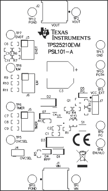
GUID-20210330-CA0I-VGBZ-S3JQ-GTN7ZL4SQ1RD-low.gifGUID-20210330-CA0I-XGSH-NVCQ-SPXCNVDPMLPN-low.gifFigure 6-1 TPS25210EVM Board (a) Top Assembly (b) Bottom Assembly
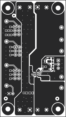
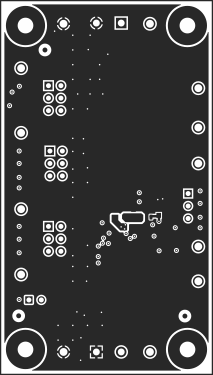
GUID-20210330-CA0I-RKLG-V5MH-8B2CVPXDTJNT-low.gifGUID-20210330-CA0I-VZP6-QQHJ-P8F16JCCBTQ5-low.gifFigure 6-2 TPS25210EVM Board (a) Top Layer (b) Bottom Layer