SLWU087E november 2013 – june 2023
- 1
- High Speed Data Converter Pro GUI
- Trademarks
- 1 Introduction
- 2 Software Start up
-
3 User Interface
- 3.1
Toolbar
- 3.1.1 File Options
- 3.1.2 Instrument Options
- 3.1.3 Data Capture Option
- 3.1.4
Test Options
- 3.1.4.1 Notch Frequency Bins
- 3.1.4.2 2 Channel Display and Cursor Lock
- 3.1.4.3 Analysis Window Markers
- 3.1.4.4 X-Scale in Time
- 3.1.4.5 Y-Scale in Voltage
- 3.1.4.6 Other Frequency Options
- 3.1.4.7 NSD Marker
- 3.1.4.8 Phase Plot
- 3.1.4.9 Phase in Degree
- 3.1.4.10 Histogram
- 3.1.4.11 Disable User Popups
- 3.1.4.12 HSDC Pro Lite Version
- 3.1.5 Help
- 3.2 Status Windows
- 3.3 Mode Selection
- 3.4 Device Selection
- 3.5 Skip Configuration
- 3.6 Capture Button (ADC Mode Only)
- 3.7 Test Selection (ADC Mode only)
- 3.8 DAC Display Panel (DAC Mode only)
- 3.9 I/Q Multi-Tone Generator
- 3.1
Toolbar
- 4 ADC Data Capture Software Operation
- 5 TSW1400 Pattern Generator Operation
- 6 TSW14J58 Functional Description
- 7 TSW14J57 Functional Description
- 8 TSW14J56 Functional Description
- 9 TSW14J50 Functional Description
- 10TSW14J10 Functional Description
- A Signal Processing in High Speed Data Converter Pro
- B History Notes
- C Revision History
4.2 Testing a TSW1400EVM with an ADS62P49EVM (CMOS Interface)
This section describes the operation when testing with an ADS62P49 EVM that is configured for CMOS output interface.
- Power down the TSW1400 if an ADC EVM is not installed.
- Connect J1 and J2 of the ADS62P49 EVM to connector J1 of the TSW1400 EVM.
- Provide unpowered +5 VDC connections to J10 and return to J12 of the ADS62P49 EVM.
- Provide a 1.5 VPP 40-MHz sine-wave clock to J19 of the ADS62P49 EVM. Make sure this clock is within the frequency limits specified in the data sheet when operating in CMOS mode.
- Provide a filtered 10-MHz analog input to CH1 (J6).
- Power up the TSW1400 followed by the ADC EVM.
- Setup the ADS62P49 EVM to operate in parallel mode, offset binary parallel CMOS output, and internal reference.
- Start up the HSDC Pro GUI as described in the Software Start Up section.
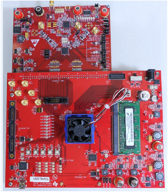
- The TSW1400 EVM connected to the CMOS connectors of the ADS62P49 EVM is shown in Figure 4-4.
 Figure 4-4 TSW1400EVM interfacing to the CMOS connectors of an ADS62P49EVM
To setup the GUI to run in the data capture mode, click on the “ADC” tab in the top left side of the GUI. Navigate to the device selection button located in the upper left side of the GUI, click on the drop down arrow, then select “ADS62p49_cmos”. After clicking on this file, a pop-up opens asking “Do you want to update the Firmware for ADC”. Click on “Yes”. The firmware starts loading which takes approximately 20 seconds to complete. After the firmware load has completed, the FPGA_CONF_DONE LED turns on after the FPGA is configured. The LEDs labeled USER_LED (0–7) should now all be on.
- Use the “Test Selection” button to change the capture display to Single Tone.
- Set the active channel setting to Channel 1/2.
- Use the default Record Length value of 65,536.
- Set the ADC Sampling Rate to 40 MHz.
- Click on the Auto Calculation of Coherent Frequency function and Rectangular capture mode if using a coherent input frequency. Otherwise, do not set this and use "Blackman" windowing mode.
- Set the input frequency source to the new value in ADC Input Target Frequency that is generated by the Auto Calculation of Coherent Frequency function.
- Make sure the display mode is set to “Frequency”.
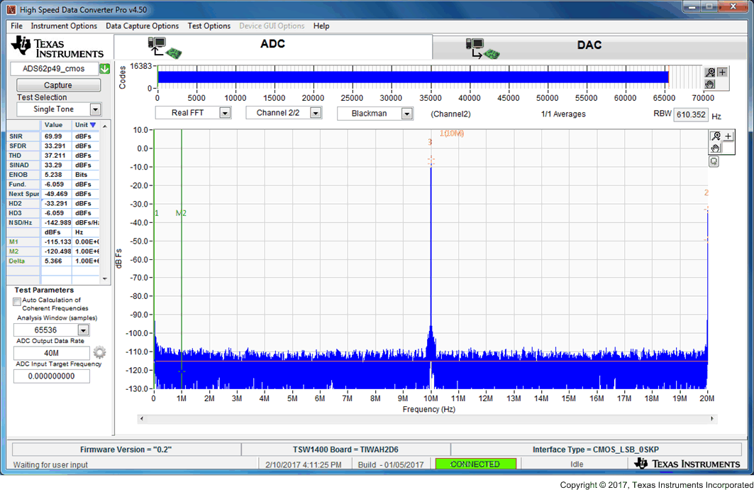
- Click on the “Capture” button to perform a data capture. The results should like similar to those shown in Figure 4-5.
 Figure 4-5 TSW1400EVM Captured Results from ADS62P49EVM