SLWU087E november   2013  – june 2023


  1.   1
  2.   High Speed Data Converter Pro GUI
  3.   Trademarks
  4. Introduction
  5. Software Start up
    1. 2.1 Installation Instructions
    2. 2.2 USB Interface and Drivers
    3. 2.3 Device ini Files
  6. User Interface
    1. 3.1 Toolbar
      1. 3.1.1 File Options
        1. 3.1.1.1 User Profiles
        2. 3.1.1.2 Resize Window
      2. 3.1.2 Instrument Options
        1. 3.1.2.1 TSW14J56 and High Speed Data Converter (HSDC) Pro Eye Quality Analysis
        2. 3.1.2.2 IO Delay
        3. 3.1.2.3 JESD204B Error Injection
        4. 3.1.2.4 FPGA Registers Write Read
      3. 3.1.3 Data Capture Option
        1. 3.1.3.1 Capture Option
        2. 3.1.3.2 Trigger Option
        3. 3.1.3.3 Using Multiple TSW14xxx and ADC EVM’s for Simultaneous Capture using Trigger Option
          1. 3.1.3.3.1 Hardware Setup
          2. 3.1.3.3.2 Setting up the Slave Board
          3. 3.1.3.3.3 Setting up the Master Board
          4. 3.1.3.3.4 Read Captured Memory from the Slave Board
      4. 3.1.4 Test Options
        1. 3.1.4.1  Notch Frequency Bins
        2. 3.1.4.2  2 Channel Display and Cursor Lock
        3. 3.1.4.3  Analysis Window Markers
        4. 3.1.4.4  X-Scale in Time
        5. 3.1.4.5  Y-Scale in Voltage
        6. 3.1.4.6  Other Frequency Options
        7. 3.1.4.7  NSD Marker
        8. 3.1.4.8  Phase Plot
        9. 3.1.4.9  Phase in Degree
        10. 3.1.4.10 Histogram
        11. 3.1.4.11 Disable User Popups
        12. 3.1.4.12 HSDC Pro Lite Version
      5. 3.1.5 Help
    2. 3.2 Status Windows
    3. 3.3 Mode Selection
    4. 3.4 Device Selection
    5. 3.5 Skip Configuration
    6. 3.6 Capture Button (ADC Mode Only)
    7. 3.7 Test Selection (ADC Mode only)
      1. 3.7.1 Single Tone FFT
        1. 3.7.1.1 Parameter Controls
        2. 3.7.1.2 ADC Captured Data Display Pane
        3. 3.7.1.3 FFT Power Spectrum
        4. 3.7.1.4 Overlay Unwrap Waveform
        5. 3.7.1.5 Single Tone FFT Statistics
      2. 3.7.2 Multi Channel Display
      3. 3.7.3 Unit Selection
      4. 3.7.4 Time Domain
      5. 3.7.5 Two Tone
      6. 3.7.6 Channel Power
    8. 3.8 DAC Display Panel (DAC Mode only)
      1. 3.8.1 Send Button (DAC Mode Only)
      2. 3.8.2 Load File to Transfer into TSW14xxx Button
      3. 3.8.3 Parameter Controls
    9. 3.9 I/Q Multi-Tone Generator
  7. ADC Data Capture Software Operation
    1. 4.1 Testing a TSW1400 EVM with an ADS5281 EVM
    2. 4.2 Testing a TSW1400EVM with an ADS62P49EVM (CMOS Interface)
  8. TSW1400 Pattern Generator Operation
    1. 5.1 Testing a TSW1400 EVM with a DAC3152 EVM
    2. 5.2 Loading DAC Firmware
    3. 5.3 Configuring TSW1400 for Pattern Generation
    4. 5.4 Testing a TSW1400 EVM with a DAC5688EVM (CMOS Interface)
  9. TSW14J58 Functional Description
    1. 6.1 Testing the TSW14J58 EVM with an ADC12DJ3200 EVM
  10. TSW14J57 Functional Description
    1. 7.1 Testing the TSW14J57 EVM with an ADC34J45 EVM
  11. TSW14J56 Functional Description
    1. 8.1 Testing the TSW14J56 EVM with an ADC34J45 EVM
  12. TSW14J50 Functional Description
    1. 9.1 Device Selection
  13. 10TSW14J10 Functional Description
    1. 10.1 DAC and ADC GUI Configuration File Changes When Using a Xilinx Development Platform
    2. 10.2 DAC38J84EVM GUI Setup Example
  14.   A Signal Processing in High Speed Data Converter Pro
    1.     A.1 Introduction
    2.     A.2 FFT Calculation from Time Domain Data
      1.      A.2.1 FFT Window Correction Factor
    3.     A.3 FFT Filtering
    4.     A.4 Single Tone Parameters
      1.      A.4.1 Number of Neighboring Bins for each FFT Window
    5.     A.5 Fundamental Power
      1.      A.5.1 Harmonic Distortions
      2.      A.5.2 SNR
      3.      A.5.3 SFDR
      4.      A.5.4 THD
      5.      A.5.5 SINAD
      6.      A.5.6 ENOB
      7.      A.5.7 Next Spur
    6.     A.6 Two Tone Parameters
    7.     A.7 Average FFT Calculation
    8.     A.8 NSD Calculation
  15.   B History Notes
  16.   C Revision History

FPGA Registers Write Read

The FPGA Registers Write Read menu option (shown in Figure 3-8) allows the user to write/read the registers of the FPGA Firmware. The firmware register map of the TSW14xxx board is loaded and the Register Name, Register Address, R/W Mode, Register Values and Register Description is shown. The register write operation is done by selecting the required register element from the tree or by specifying the required register address in the "Address" input control and providing a value to be written at "Write Data" input control and then clicking on the "Write Register" button. Similarly, the register read operation is done by clicking on the "Read Register" button after specifying the required register address and the read register value are updated both in the register tree and "Read Data" output indicator. The current register configuration listed in the register map is exported as “.cfg” file by using the “Save Config” button and the same is loaded by using the “Load Config” button. The “Load Config” operation overwrites the existing data in registers with the value specified in the loaded configuration file.
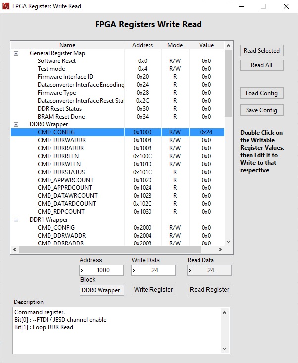
GUID-20210414-CA0I-MV0G-P7JP-FXTFVS0MMDKN-low.png Figure 3-8 FPGA Registers Write Read Window
Note: This feature is currently implemented only for the TSW14J58EVM.