SNAA378 January 2023 LMX1204
3.4 Phase Error Across all LMX1204 Channels
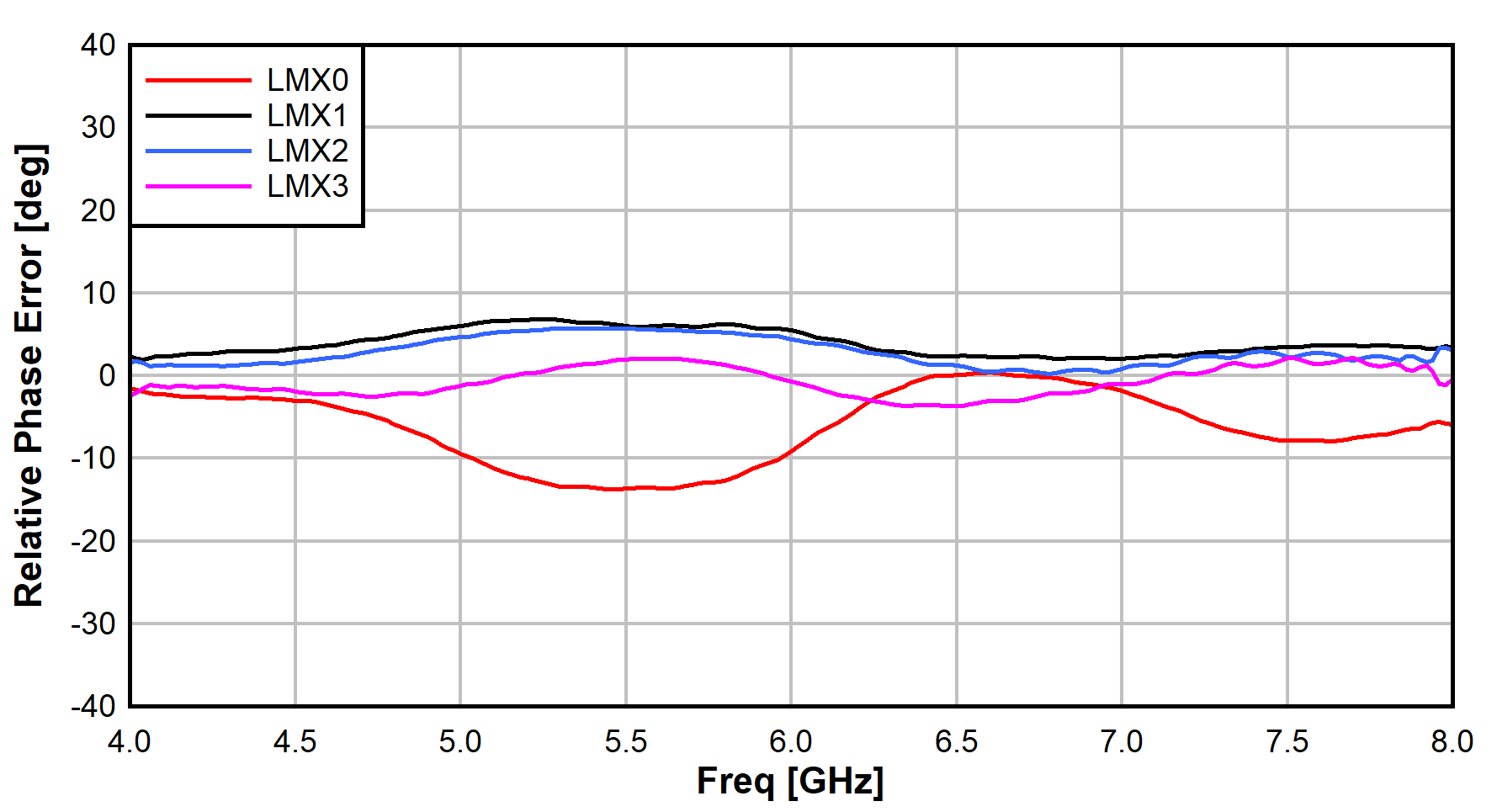
Figure 3-4 shows the phase error relative to the overall average between all output channels of the lower level LMX1204 devices comprising a total of 16 channels. This variation includes output trace and cables as the previous case in addition to the root LMX1204 device variation and feed traces. The phase error in this situation is also very consistent across all channels with LMX0 device being a small outlier. This is likely due to trace routing on the board and having to transition between the top and bottom layer for that device.
 Figure 3-4 Relative Phase Error Across
Channels Over Multiple LMX1204 Devices