SNOAA79 June 2021 DAC121S101QML-SP , LMP7704-SP , TPS7A4501-SP
Design Description
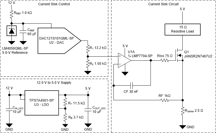
Voltage controlled current sinks are an integral part of many current-controlled space applications. One of its most popular applications is adjustable-current, laser diode drivers which are often used in laser communications systems (also known as optical inter-satellite links (OISL)). The circuit is also seen in other applications like LiDAR which might benefit from laser diodes. It consists of three main elements: the sense resistor (RSense), an N-channel MOSFET (Q1), and an operational amplifier (op amp) that controls the MOSFET.
The basic operating principle of the circuit starts with current flowing through the load from a voltage supply (in this case 5 V). As current flows through the load, a voltage is developed on RSense. The op amp uses the sensed voltage as feedback and drives its output until the sensed voltage is equal to the DAC output (non-inverting input). In this case, Q1 is operated in the linear region and serves as a voltage-controlled resistance. The components: Riso, CF, and RF are used to compensate the circuit and ensure stable operation.