SNVA964 June 2020 LP8866-Q1
2.4 Layout Consideration
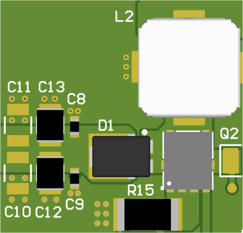
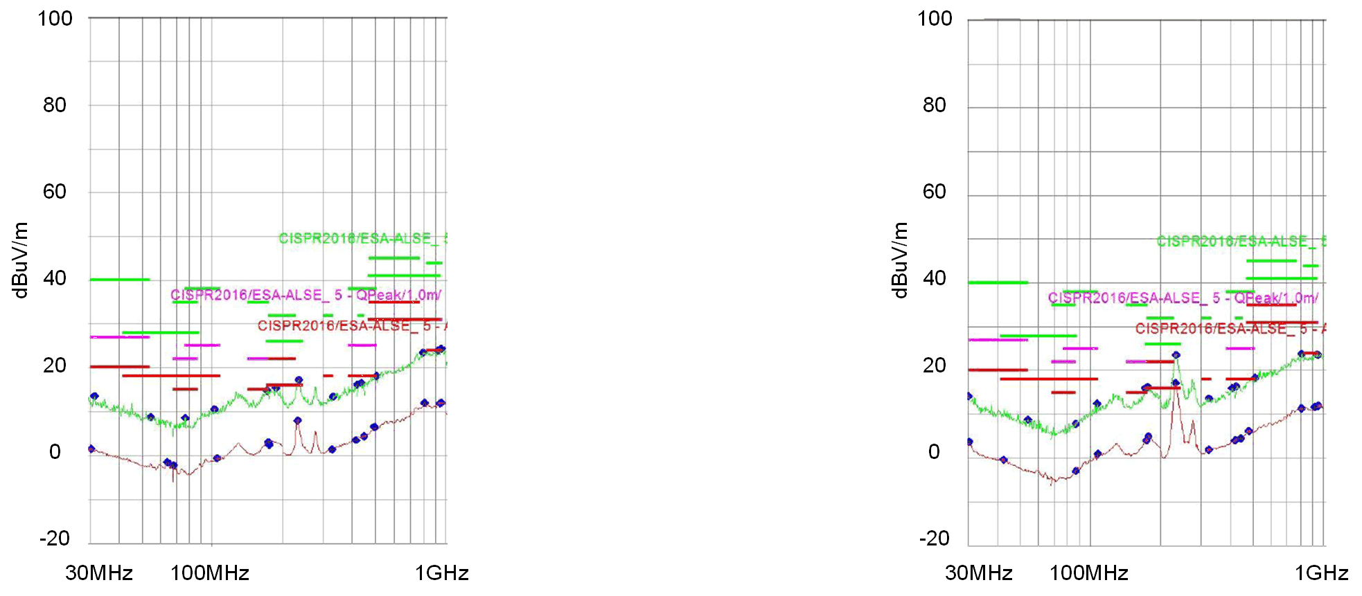
A optimized layout is crucial for EMI reduction. Critical current loops need to be minimized. Minimum loop area for high frequencies can be achieved when return current flows in the ground plane just under the top-layer power traces, if the ground plane is intact under these traces. So a solid internal plane for ground (return) should be built. To minimize the current loop for high frequencies, put a small high-frequency capacitor as near as possible to the boost diode. And place vias to internal ground planes close to the capacitors' GND pin, as shown in Figure 13. An experiment is performed to place C8 and C9, two 10-nF high-frequency ceramic capacitors, on the footprint of C10 and C11 and the conducted/radiated emissions measurement results are compared in Figure 14 and Figure 15.
 Figure 13. Boost Critical Loop Layout
| (a) C8 and C9 in original position | (b) C8 and C9 on footprint of C10 and C11 |

| (a) C8 and C9 in original position | (b) C8 and C9 on footprint of C10 and C11 |