SNVA964 June 2020 LP8866-Q1
2.3 LED Current Sink Capacitors
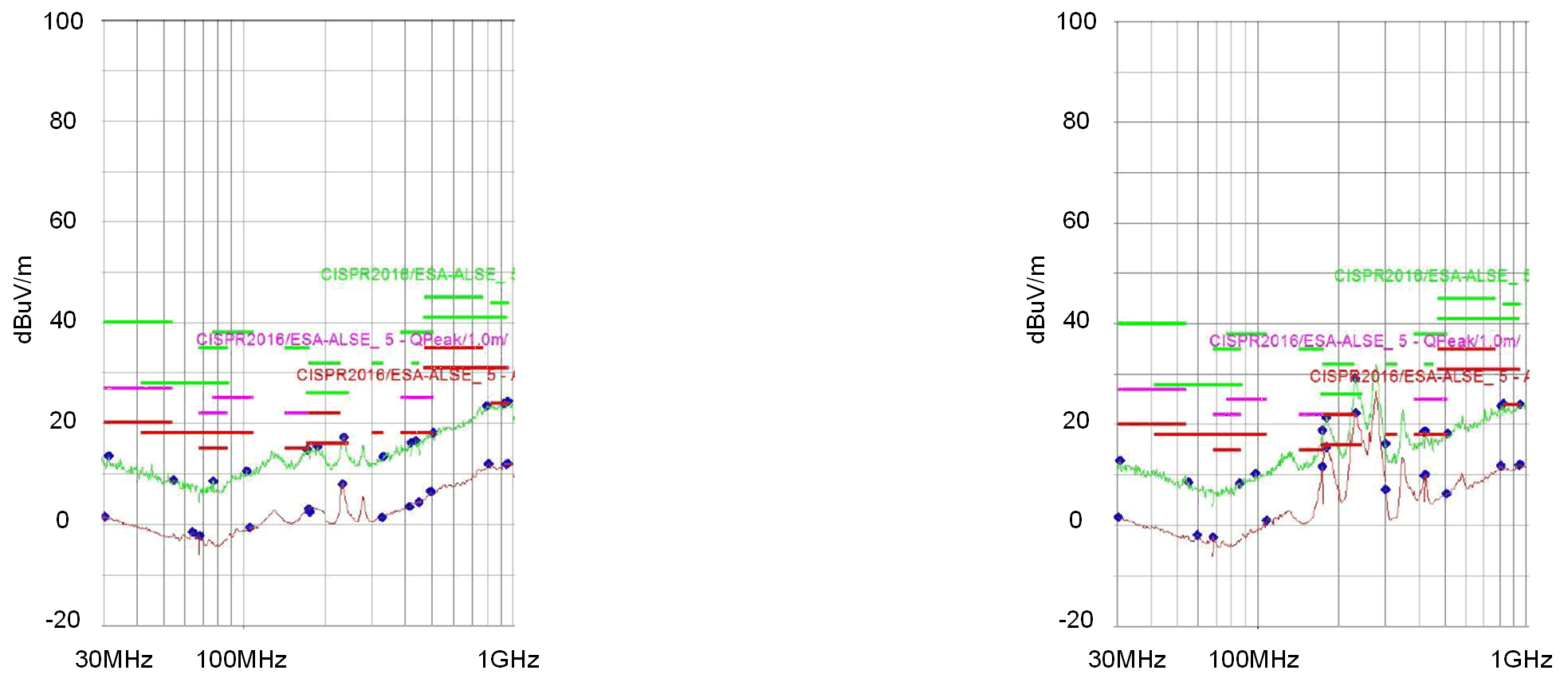
Since the LED driver board is connected to the LED load with a 20-cm long wire harness, these wires can act as efficient antennas in the region of a few hundred MHz. It is of high importance to place bypass capacitors close to the connector on the LED driver board to prevent the wires from radiating noise. A 1-nF capacitor is recommended to be placed at each LP8866-Q1 OUTx pin to ground. Figure 11 and Figure 12 show a substantial improvement in EMI with these capacitors.

| (a) With 1-nF capacitors
from current sinks to ground |
(b) Without 1-nF capacitors
from current sinks to ground |

| (a) With 1-nF capacitors
from current sinks to ground |
(b) Without 1-nF capacitors
from current sinks to ground |