SNVU839 November 2022 LP8758-B0 , LP8758-E0 , LP8758-E3 , LP8758-EA
1.2 Module Design Details
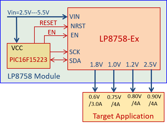
The module is designed as a castellated PCB module. It is composed of a PMIC LP8758-Ex (or any Ex variant) which has 4 single-phase bucks, and a simple and low cost MCU PIC16F15223. The LP8758-Ex PMIC has no output because the "EN" pin is pull-down by the MCU at power up moment. The MCU starts its built-in program to reconfigure the PMIC through its I2C port. After reconfiguration is done, the MCU raises up the "EN" and "RESET" pins to allow the PMIC to start its power on sequence; all 4 PMIC power rails will power up according to the customers' application needs which is implemented by the MCU program.
 Figure 1-1 Block Diagram
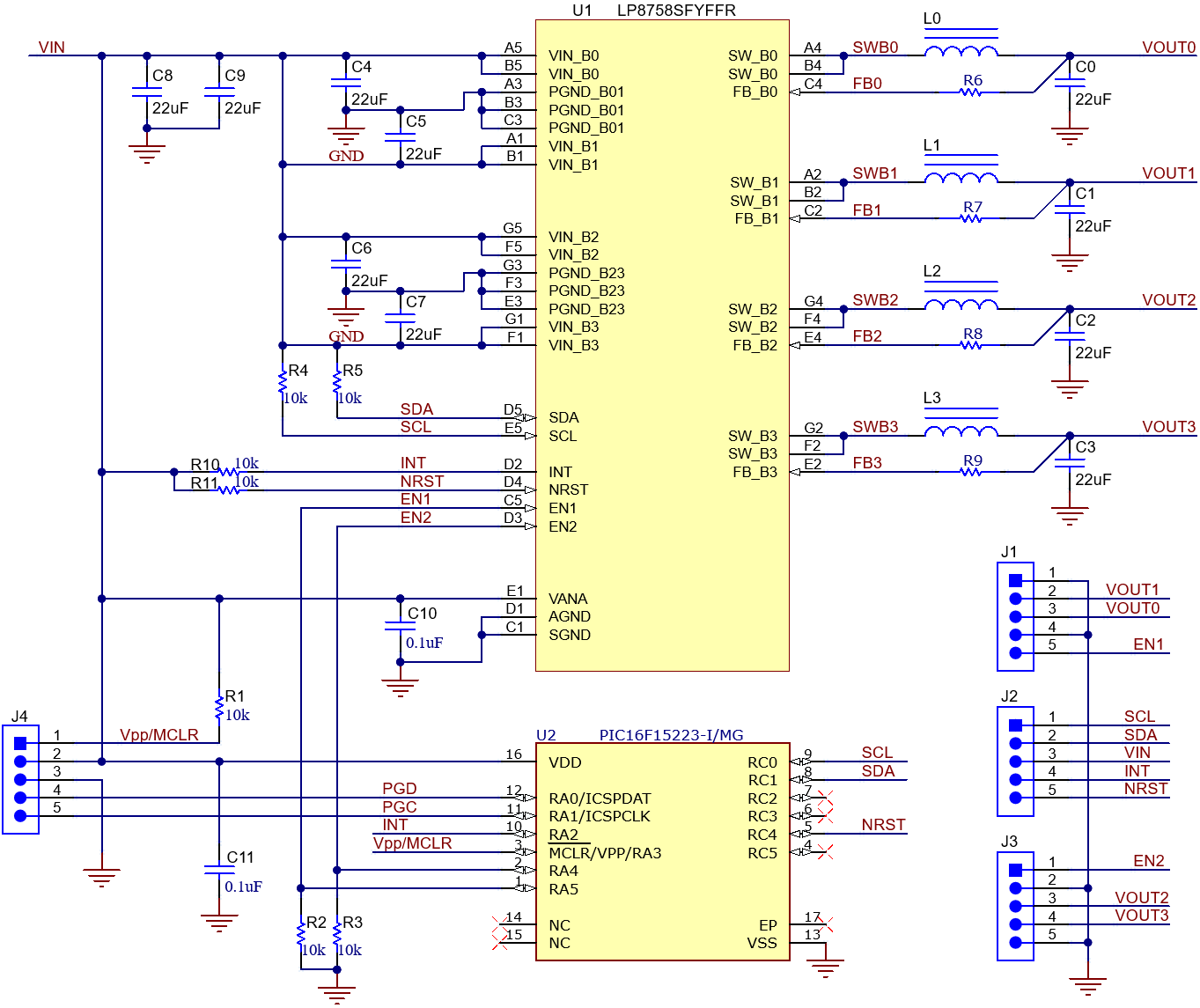
Schematics of the module as shown by the figure below.
 Figure 1-2 Module Schematic
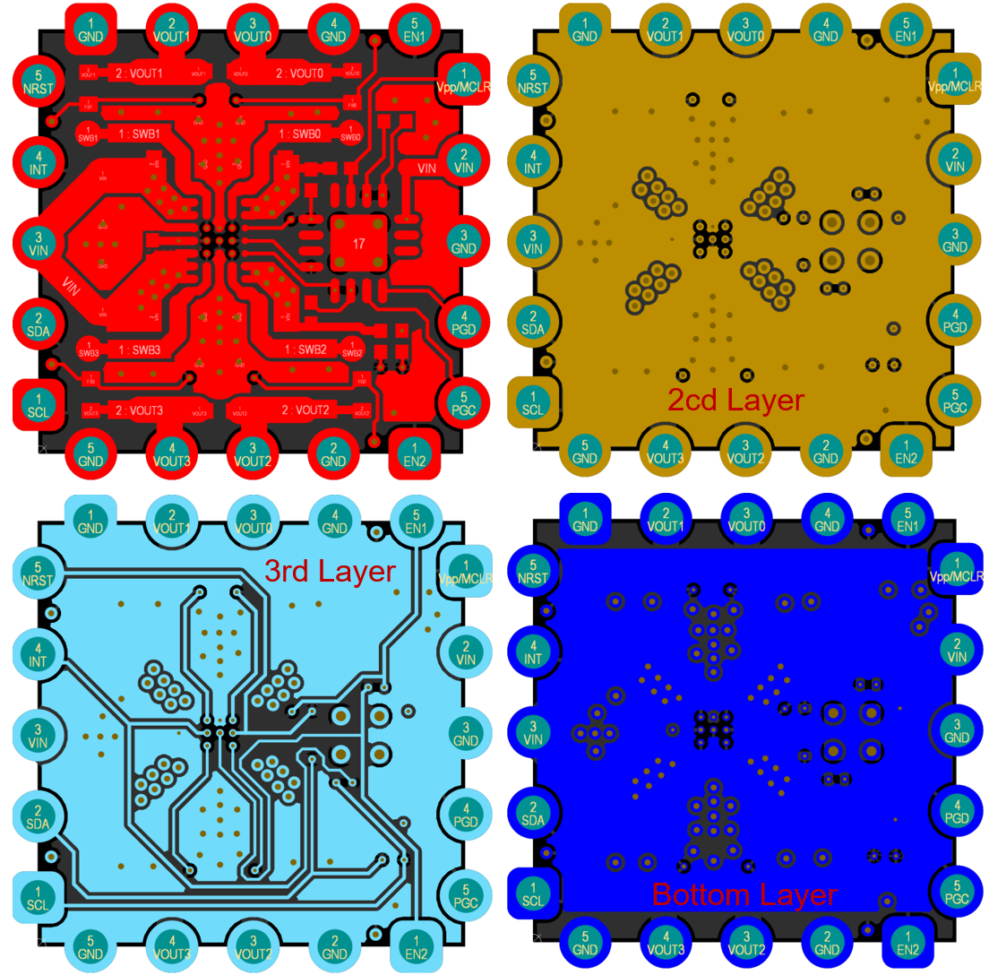
4 PCB layers of the module as shown by the figure below.
 Figure 1-3 4 PCB Module Layers
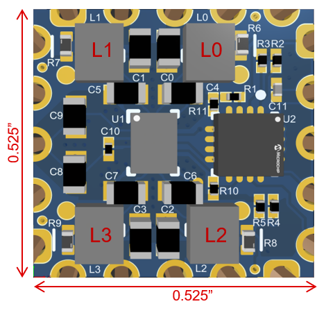
Measurement of the module as shown by the figure below.
 Figure 1-4 Module Measurement