SPRAD61A March   2023  – November 2023 AM2732 , AM2732 , AM2732-Q1 , AM2732-Q1


  1.   1
  2.   Abstract
  3.   Trademarks
  4. Introduction
    1. 1.1 Acronyms
  5. Power
    1. 2.1 Discrete DC-DC Power Solution
    2. 2.2 Integrated PMIC Power Solution
    3. 2.3 Power Decoupling and Filtering
    4. 2.4 Power Consumption
  6. Clocking
    1. 3.1 Crystal and Oscillator Input Options
    2. 3.2 Output Clock Generation
    3. 3.3 Crystal Selection and Shunt Capacitance
    4. 3.4 Crystal Placement and Routing
  7. Resets
  8. Bootstrapping
    1. 5.1 SOP Signal Implementation
    2. 5.2 QSPI Memory Controller Implementation
    3. 5.3 ROM QSPI Boot Requirements
  9. JTAG Emulators and Trace
  10. Multiplexed Peripherals
  11. Digital Peripherals
    1. 8.1 General Digital Peripheral Routing Guidelines
  12. Layer Stackup
    1. 9.1 TMDS273GPEVM Layer Stackup
      1. 9.1.1 TMDS273GPEVM Key Stackup Features
    2. 9.2 Four Layer ZCE Example Layer Stackup
      1. 9.2.1 ZCE Four Layer Example Key Stackup Features
    3. 9.3 Four Layer NZN Example Layer Stackup
      1. 9.3.1 NZN Four Layer Example Key Stackup Features
  13. 10Vias
  14. 11BGA Power Fan-Out and Decoupling Placement
    1. 11.1 Ground Return
      1. 11.1.1 Ground Return - TMDS273GPEVM
      2. 11.1.2 Ground Return - ZCE Four Layer Example
      3. 11.1.3 Ground Return - NZN Four Layer Example
    2. 11.2 1.2 V Core Digital Power
      1. 11.2.1 1.2 V Core Digital Power Key Layout Considerations
        1. 11.2.1.1 1.2V Core Layout - TMDS273GPEVM
        2. 11.2.1.2 1.2V Core Layout - ZCE Four Layer Example
        3. 11.2.1.3 1.2V Core Layout - NZN Four Layer Example
    3. 11.3 3.3 V Digital and Analog Power
      1. 11.3.1 3.3 V Digital and Analog Power Key Layout Considerations
        1. 11.3.1.1 3.3V Digital and Analog Layout - TMDS273GPEVM
        2. 11.3.1.2 3.3V Digital and Analog Layout - ZCE Four Layer Example
        3. 11.3.1.3 3.3V Digital and Analog Layout - NZN Four Layer Example
    4. 11.4 1.8 V Digital and Analog Power
      1. 11.4.1 1.8 V Digital and Analog Power Key Layout Considerations
        1. 11.4.1.1 1.8V Digital and Analog Layout - TMDS273GPEVM
        2. 11.4.1.2 1.8V Digital and Analog Layout - ZCE Four Layer Example
        3. 11.4.1.3 1.8V Digital and Analog Layout - NZN Four Layer Example
  15. 12References
  16. 13Revision History

Integrated PMIC Power Solution

The AM273x GP EVM integrates a Power Management Integrated Circuit (PMIC) based power solution that may be used as a reference solution for some systems. The solution consists of a LM63625 voltage converter pre-regulator and a LP877451 PMIC to generate the MCU core, SRAM, system digital and analog I/O power. A TPS73501 Low Drop Out (LDO) regulator is used for the Ethernet PHY.

The power good generation circuits available on the PMIC and DC-DC regulators should be combined to a single line and used to drive the reset (nRESET) of the AM273x device.
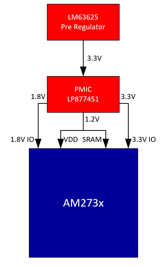
GUID-4970C545-8563-484F-9296-B7D5BFA9BA90-low.png Figure 2-1 AM273x PMIC Example Solution
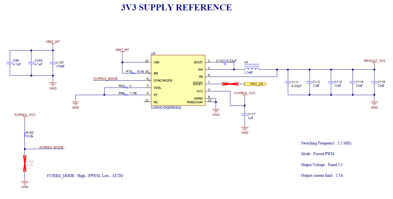
GUID-016BCDD8-39BA-4D17-B745-727386AED915-low.png Figure 2-2 AM273x PMIC 3.3V Pre-Regulator Implementation
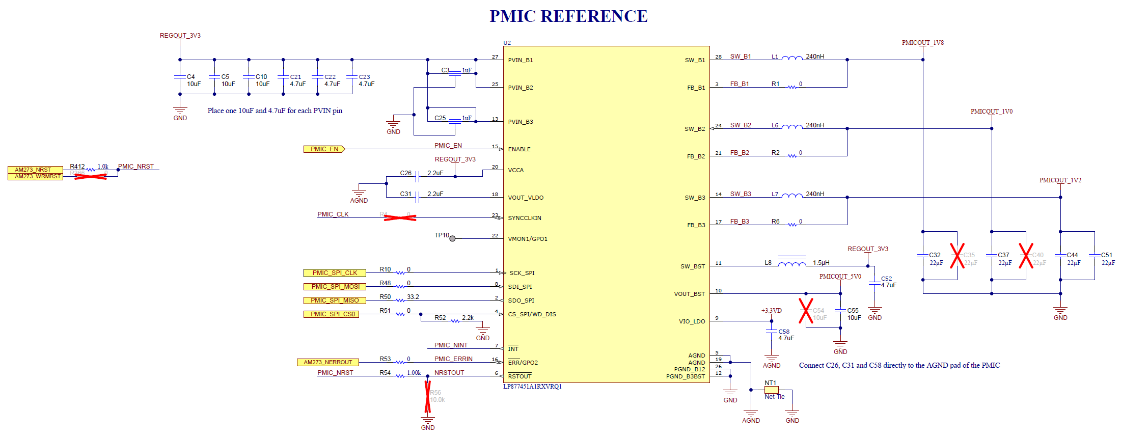
GUID-AEC98080-7858-4B8F-BF2E-F99B85088474-low.png Figure 2-3 AM273x PMIC Implementation