SPRUIT1B May   2020  – November 2020


  1.   Trademarks
  2. 1Introduction
    1. 1.1 Key Features
  3. 2GESI Expansion Board Overview
    1. 2.1 GESI Expansion Board Identification
    2. 2.2 GESI Expansion Board Component Identification
  4. 3GESI Expansion Board - User Setup/Configuration
    1. 3.1 GESI Infotainment Expansion Board With CP Board
      1. 3.1.1 Board Assembly Procedures
    2. 3.2 Power Requirements
    3. 3.3 EVM Reset/Interrupt Push Buttons
    4. 3.4 EVM Configuration DIP Switch
  5. 4GESI Expansion Board Hardware Architecture
    1. 4.1  GESI Expansion Board Hardware Top Level Diagram
    2. 4.2  Expansion Connectors
    3. 4.3  Board ID EEPROM
    4. 4.4  Ethernet Interface
      1. 4.4.1 RGMII Clocking Scheme
      2. 4.4.2 Ethernet Port LED Indication
    5. 4.5  PROFI BUS / RS485
    6. 4.6  LIN Interface
    7. 4.7  MCAN
    8. 4.8  MUX Selection
      1. 4.8.1 MUX – PRGx_MDIO/MDC, CPSW9G_MDIO/MDC
      2. 4.8.2 MUX – PRG1_RGMII1/PRG1_PWM
      3. 4.8.3 MUX – PRG1_PWM/MCAN
      4. 4.8.4 MUX_MC/BP_SEL
    9. 4.9  GESI LaunchPad-Booster Pack Interface
    10. 4.10 Motor Control Interface
    11. 4.11 USS/IMU Header
    12. 4.12 Test Header
  6.   A Interface Mapping
  7.   B GESI Board GPIO Mapping
  8.   C I2C Address Mapping
  9.   D Revision History

USS/IMU Header

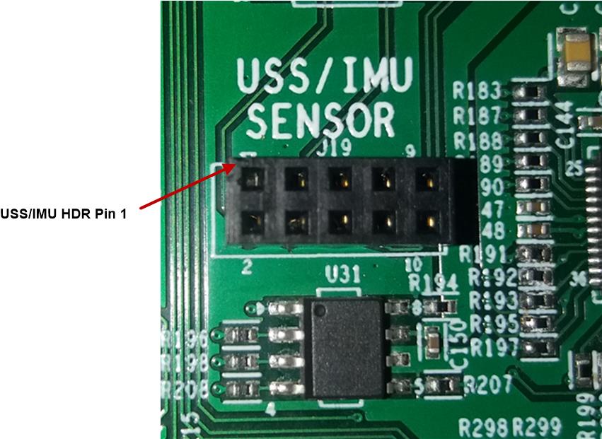
Table 4-9 contains the pin out details of USS/IMU header. USS/IMU Header on GESI Expansion Board is shown in Figure 4-18.

Table 4-9 Pin Outs of J19 (USS/IMU Header) Connector
Pin outs of J19
PinNet Name
1I2C5_SDA
2UART3_TX
3I2C5_SCL
4UART3_RX
5DGND
6DGND
7IMU_GPIO0
8UART3_RTSn
9IMU_GPIO1
10UART3_CTSn
GUID-08F218F4-7517-49A4-9E5F-99851BD7B6BB-low.jpgFigure 4-18 USS/IMU Header