SPRUJ12F August 2021 – January 2024 AM2431 , AM2432 , AM2434
- 1
- Abstract
- Trademarks
- 1Preface: Read This First
- 2Kit Overview
- 3Board Setup
-
4Hardware Description
- 4.1 Functional Block Diagram
- 4.2 BoosterPack Headers
- 4.3 GPIO Mapping
- 4.4 Reset
- 4.5 Clock
- 4.6 Memory Interface
- 4.7 Ethernet Interface
- 4.8 USB 2.0 Interface
- 4.9 I2C Interface
- 4.10 Industrial Application LEDs
- 4.11 UART Interface
- 4.12 eQEP Interface
- 4.13 CAN Interface
- 4.14 FSI Interface
- 4.15 JTAG Emulation
- 4.16 Test Automation Interface
- 4.17 SPI Interface
- 5References
- A E3 Design Changes
- B Revision A Design Changes
- Revision History
4.7 Ethernet Interface
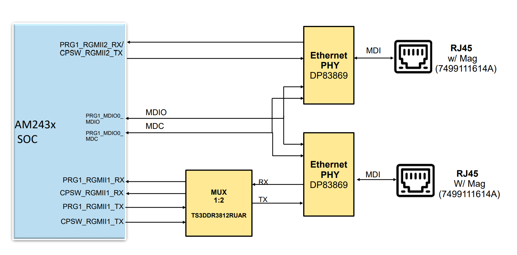
The LaunchPad supports two Ethernet PHYs that are terminated to RJ45 connectors with integrated magnetics for external communication.
 Figure 4-9 Ethernet Connection
The 48 pin PHY (DP83869) is configured to advertise gigabit operation with the internal delay set to accommodate the internal delay of the AM243x SoC.
The first PHY is interfaced to the PRG1/CPSW RGMII2 ports of the SoC that are internally multiplexed in the SoC and the MDI interface from the same PHY is terminated to a RJ45 connector with integrated magnetics.
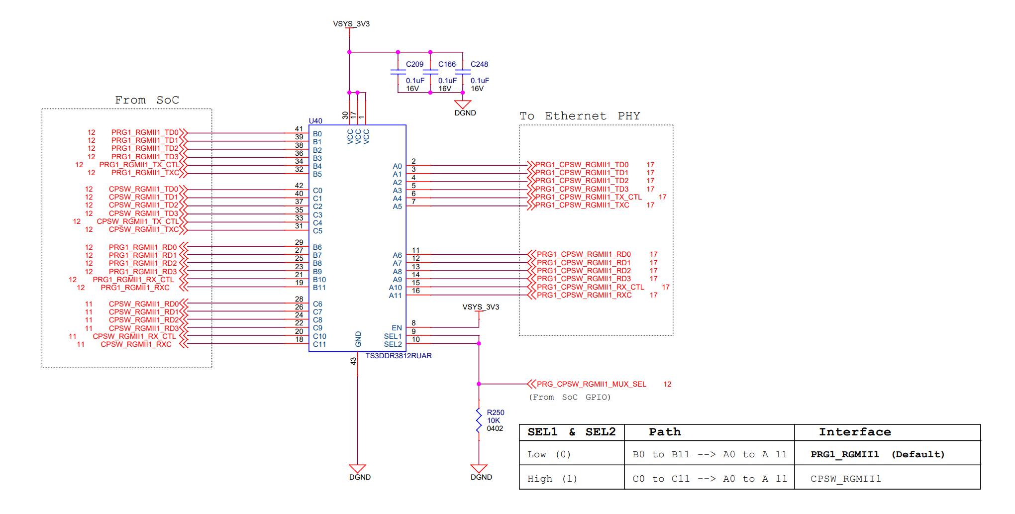
The second PHY is interfaced to the PRG1/CPSW RGMII1 ports of the SoC that are multiplexed using an external on-board MUX whose select line is be controlled from a GPIO (PRG_CPSW_RGMII1_MUX_SEL) of the SoC and the MDI interface from the same PHY is terminated to a RJ45 connector with integrated magnetics. A 1:2 mux (TS3DDR3812RUAR) is used to select between the PRG1 and CPSW RGMII1 ports.
 Figure 4-10 CPSW or PRG RGMII1 Ethernet
Data Mux
Figure 4-10 CPSW or PRG RGMII1 Ethernet
Data MuxTo select between the PRG and CPSW operation for both PHYs, the MDIO and MDC signals, which are internally multiplexed in the SoC, must be selected from each controller.
Two RJ45 connectors with integrated magnetics and status LEDs (7499111614A from Wurth) are used on the board for Ethernet 10Mb/100Mb/1Gb connectivity.