SPRUJA2 November   2023


  1.   1
  2.   Description
  3.   Get Started
  4.   Features
  5.   5
  6. 1Evaluation Module Overview
    1. 1.1 Introduction
    2. 1.2 Kit Contents
    3. 1.3 Device Information
    4. 1.4 Specification
  7. 2Hardware
    1. 2.1  Additional Images
    2. 2.2  Key Features
      1. 2.2.1 Processor
      2. 2.2.2 Power Supply
      3. 2.2.3 Memory
      4. 2.2.4 JTAG/Emulator
      5. 2.2.5 Supported Interfaces and Peripherals
      6. 2.2.6 Expansion Connectors/Headers
    3. 2.3  Interface Mapping
    4. 2.4  Power ON/OFF Procedure
      1. 2.4.1 Power ON Procedure
      2. 2.4.2 Power OFF Procedure
      3. 2.4.3 Test Points
    5. 2.5  Clocking
      1. 2.5.1 Peripheral Ref Clock
    6. 2.6  Reset
    7. 2.7  CSI Interface
    8. 2.8  OLDI Interface
    9. 2.9  DSI Interface
    10. 2.10 Audio Codec Interface
    11. 2.11 HDMI Display Interface
    12. 2.12 JTAG Interface
    13. 2.13 Test Automation Header
    14. 2.14 UART Interface
    15. 2.15 USB Interface
      1. 2.15.1 USB 2.0 Type A Interface
      2. 2.15.2 USB 2.0 Type C Interface
    16. 2.16 Memory Interfaces
      1. 2.16.1 LPDDR4 Interface
      2. 2.16.2 OSPI Interface
      3. 2.16.3 MMC Interfaces
        1. 2.16.3.1 MMC0 - eMMC Interface
        2. 2.16.3.2 MMC1 - Micro SD Interface
        3. 2.16.3.3 MMC2 - M.2 Key E Interface
      4. 2.16.4 Board ID EEPROM
    17. 2.17 Ethernet Interface
      1. 2.17.1 CPSW Ethernet PHY Strapping
      2. 2.17.2 CPSW Ethernet PHY1 Default Configuration
      3. 2.17.3 CPSW Ethernet PHY2 Default Configuration
    18. 2.18 GPIO Port Expander
    19. 2.19 GPIO Mapping
    20. 2.20 Power
      1. 2.20.1 Power Requirement
      2. 2.20.2 Power Input
      3. 2.20.3 Power Supply
      4. 2.20.4 Power Sequencing
      5. 2.20.5 AM62P SoC Power
      6. 2.20.6 Current Monitoring
    21. 2.21 EVM User Setup/Configuration
      1. 2.21.1 DIP Switches
      2. 2.21.2 Boot Modes
      3. 2.21.3 User Test LEDs
    22. 2.22 Expansion Headers
      1. 2.22.1 User Expansion Connector
      2. 2.22.2 MCU Connector
      3. 2.22.3 GPMC NAND (x8) Connector
    23. 2.23 Interrupt
    24. 2.24 I2C Address Mapping
  8. 3Hardware Design Files
  9. 4Compliance Information
    1. 4.1 Compliance and Certifications
  10. 5Additional Information
    1. 5.1 Known Hardware or Software Issues
      1. 5.1.1 Issue 1 - Watchdog Reset
      2. 5.1.2 Issue 2 - Power Down Sequence
    2. 5.2 Trademarks

USB 2.0 Type A Interface

USB2.0 data lines DP and DM from Type A connector J9 are connected to the USB1 interface of the AM62P SOC to provide USB high-speed/full-speed communication. USB1_VBUS to the SOC is provided through a resistor divider network to support (5 V-30 V) VBUS operation. USB1_DRVVBUS from SOC controls the enable pin of a 500 mA current limited load switch Mfr Part# TPS2051BDto allow on board 5 V supply to power the VBUS. This load switch has an over current indication pin connected to I2C based GPIO expander on the SK EVM.

A common mode choke of Mfr Part# DLW21SZ900HQ2B is provided on USB Data lines for EMI/ EMC reduction along with ESD protection Mfr Part# TPD4S012DRYR to suppress any transient voltages.
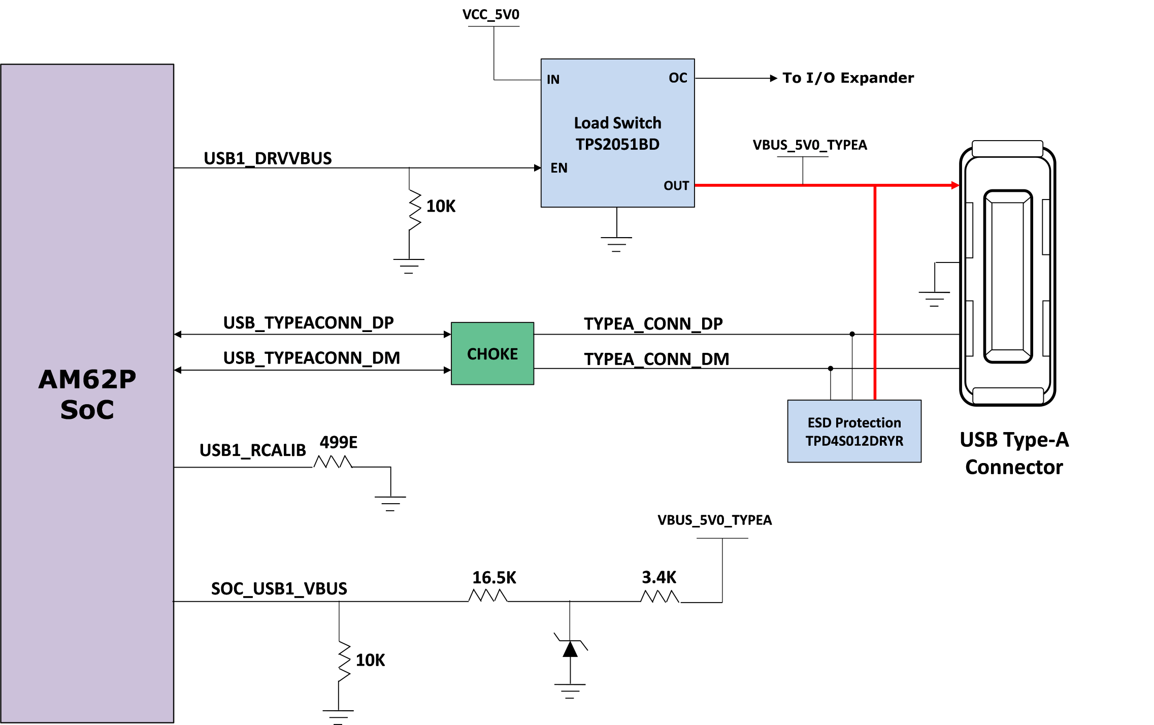
GUID-20231102-SS0I-SPVL-X8L7-7PCRLZTNJFWQ-low.png Figure 2-15 USB 2.0 Type A Interface