SPRUJA2 November 2023
- 1
- Description
- Get Started
- Features
- 5
- 1Evaluation Module Overview
-
2Hardware
- 2.1 Additional Images
- 2.2 Key Features
- 2.3 Interface Mapping
- 2.4 Power ON/OFF Procedure
- 2.5 Clocking
- 2.6 Reset
- 2.7 CSI Interface
- 2.8 OLDI Interface
- 2.9 DSI Interface
- 2.10 Audio Codec Interface
- 2.11 HDMI Display Interface
- 2.12 JTAG Interface
- 2.13 Test Automation Header
- 2.14 UART Interface
- 2.15 USB Interface
- 2.16 Memory Interfaces
- 2.17 Ethernet Interface
- 2.18 GPIO Port Expander
- 2.19 GPIO Mapping
- 2.20 Power
- 2.21 EVM User Setup/Configuration
- 2.22 Expansion Headers
- 2.23 Interrupt
- 2.24 I2C Address Mapping
- 3Hardware Design Files
- 4Compliance Information
- 5Additional Information
2.8 OLDI Interface
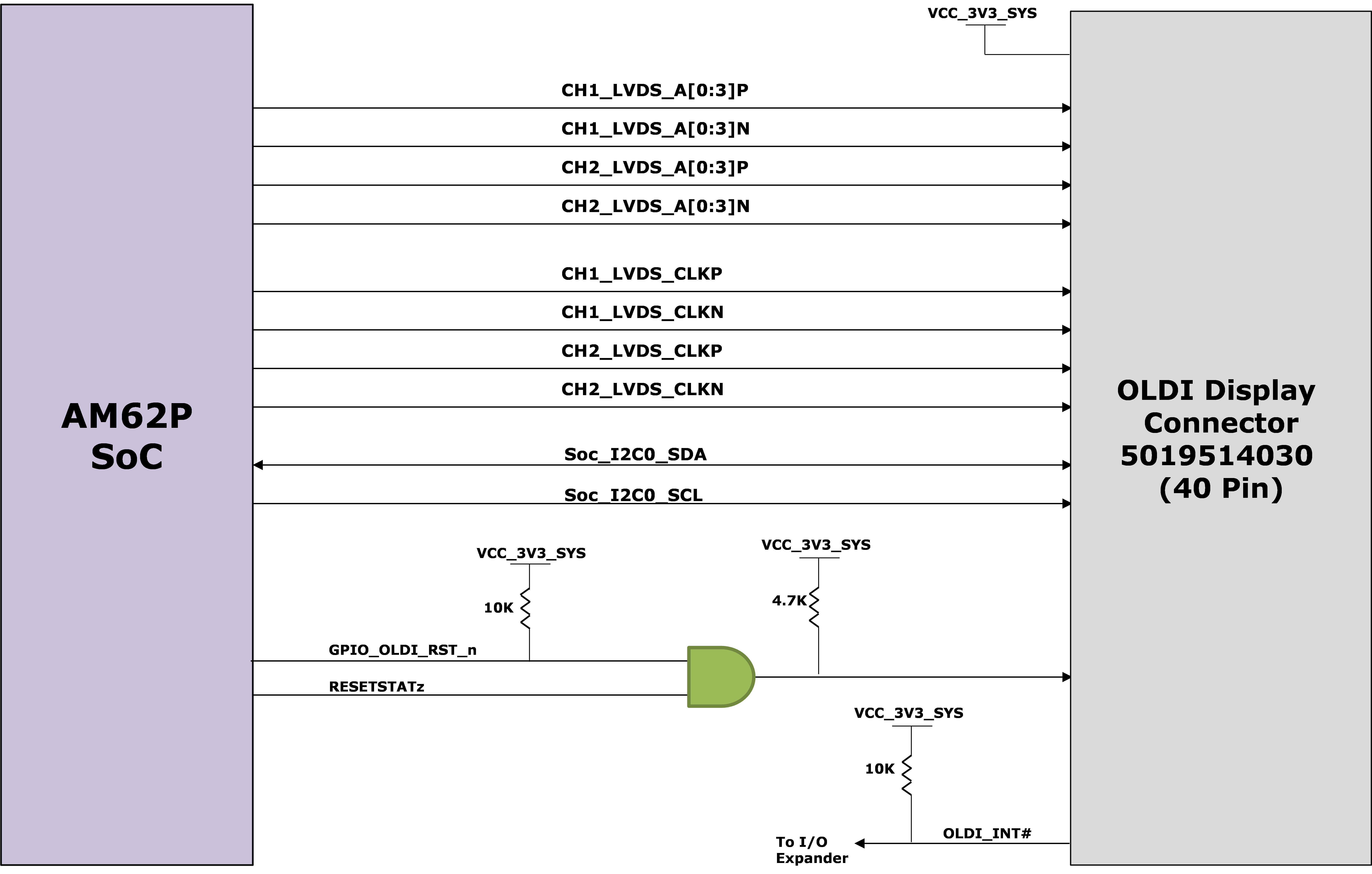
The OLDI0 Display interface of the AM62P SOC is connected to a 40 pin LVDS display connector (J27) Mfr Part# 5019514030 from Molex. The AM62P SK EVM supports dual channel 8-bit LVDS output with resolutions up to 3840x1080p. Apart from the dual channel LVDS signals, the 40-pin connector is provided with a 3.3V supply with sourcing capability until 500 mA, I2C0 for any pre-initializations and two GPIO’s for handling interrupt and reset to the interfacing display.
 Figure 2-8 OLDI Interface
Table 2-5 OLDI Display Connector (J27)
Pinout
| Pin No. | Signal | Pin No. | Signal |
|---|---|---|---|
| 1 | DGND | 21 | CH1_LVDS_A2N |
| 2 | CH2_LVDS_A3P | 22 | DGND |
| 3 | CH2_LVDS_A3N | 23 | CH1_LVDS_CLKP |
| 4 | DGND | 24 | CH1_LVDS_CLKN |
| 5 | CH2_LVDS_A2P | 25 | DGND |
| 6 | CH2_LVDS_A2N | 26 | CH1_LVDS_A1P |
| 7 | DGND | 27 | CH1_LVDS_A1N |
| 8 | CH2_LVDS_CLKP | 28 | DGND |
| 9 | CH2_LVDS_CLKN | 29 | CH1_LVDS_A0P |
| 10 | DGND | 30 | CH1_LVDS_A0N |
| 11 | CH2_LVDS_A1P | 31 | DGND |
| 12 | CH2_LVDS_A1N | 32 | OLDI_INT# |
| 13 | DGND | 33 | OLDI_RESETN |
| 14 | CH2_LVDS_A0P | 34 | DGND |
| 15 | CH2_LVDS_A0N | 35 | DGND |
| 16 | DGND | 36 | NC |
| 17 | CH1_LVDS_A3P | 37 | NC |
| 18 | CH1_LVDS_A3N | 38 | SOC_I2C0_SDA |
| 19 | DGND | 39 | SOC_I2C0_SCL |
| 20 | CH1_LVDS_A2P | 40 | VCC_3V3_SYS_CONN |