SWRA680 November 2020 CC3100 , CC3120 , CC3135 , CC3200 , CC3220R , CC3220S , CC3220SF , CC3235S , CC3235SF
3.2 Load Capacitance
The load capacitance (CL) refers to the net capacitance in the oscillator feedback loop. The correct load capacitance is essential to ensure the oscillation frequency of the crystal is within the expected range. The load capacitance is equal to the amount of capacitance seen between the crystal pins, and it includes the shunt capacitors added on the board, the PCB trace parasitic capacitance, the component pad capacitance, device pin capacitance, and so forth.
 Figure 3-1 Simplified Crystal Equivalent Load
Capacitance Circuit
Figure 3-1 Simplified Crystal Equivalent Load
Capacitance CircuitFigure 3-2 illustrates a typical crystal oscillator circuit and sources of load capacitance. The total load capacitance includes discrete load capacitors (CL1 and CL2), device pin capacitance (CPIN), and stray board capacitance (CSTRAY). It is important to account for all sources of capacitance when calculating value for the discrete capacitor components, CL1 and CL2, in Equation 2 for a specific board design.
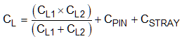
These capacitors, with any parasitic capacitance in the PCB and the crystal terminals, compose the total load capacitance (CL) that helps set the crystal resonance frequency. The crystal data sheet provides the optimum load capacitance CL for the crystal. This total CL typically consists of both the loading capacitors and the parasitic capacitance of the layout and packaging.
The following presents the relative advantages of crystals with different CL values. The disadvantages of lower CL are as follows:
- Crystals with CL < 8-pF are more difficult to source with short lead times
- Frequency becomes more sensitive to changes in board capacitance as CL decreases.
- Lowering CL results in degraded RF phase noise.
Advantages of lower CL are as follows:
- Lower CL causes a much faster start-up time. (Start-up time goes as )
- Lower CL causes a faster amplitude control loop response time.
- Lower CL makes it easier to use small size crystals (2.0 × 1.6 and so on) and maintain a start-up time at or less than 400 μs. Start-up time worsens with smaller crystals due to an increase in LM.