TIDA035 October 2020
2 Two-point Insulation Resistance Measurements
If the isolation leakage errors happen at both positive terminal and negative terminal of a high-voltage battery, the circuit diagram is as shown in Figure 2-1. Here, RISOP represents the parasitic insulation resistance between high-voltage battery positive terminal and chassis ground, while RISON represents the parasitic insulation resistance between high-voltage battery negative terminal and chassis ground. In accordance with TIDA-01513 specification, S1 and S2 are control switches for positive terminal and negative terminal respectively. Rps (Replace Rps1+Rps2 for simplicity) and Rns (Replace Rns1+Rns2 for simplicity) are series resistors in positive terminal and negative terminal respectively. Rs1 and Rs2 are sampling resistors across op-amp. ISO_POS and ISO_NEG are measured by analog-digital converter for signal processing. Additionally, the battery voltage needs to be measured in order to accomplish the entire insulation resistance measurement. In TIDA-01513, AMC1301-Q1 device is used to perform this measurement and provide an isolated signal for analog-digital converter.
 Figure 2-1 Isolation Errors at Both Positive and
Negative Terminals
Figure 2-1 Isolation Errors at Both Positive and
Negative TerminalsWhen only S1 is closed, there are two leakage current paths for the high-voltage battery. One leakage current flows from the positive terminal of high-voltage battery (junction a) to chassis ground, and depends on the positive terminal voltage (referred to chassis ground) and RISOP. The other leakage current, which goes through high-voltage battery, flows from the negative terminal of high-voltage battery (junction b) to chassis ground, and depends on the negative terminal voltage (referred to chassis ground) and RISON.
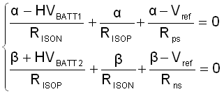
According to Kirchhoff’s Current Law, the sum of currents entering and leaving the same junction is always zero. Equations are found at junction a and junction c respectively.
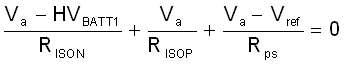
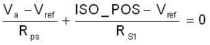
Here Va is the voltage at junction a, which is the high-battery positive terminal voltage referred to chassis ground. Vref is the reference voltage applied to op-amp non-inverting input (+). Rps is the sum of Rps1 and Rps2, that is Rps = Rps1 + Rps2. HVBATT1 is the battery voltage measured by ADC when only S1 is closed. ISO_POS is the top op-amp output voltage during the same scenario. HVBATT1 and ISO_POS should be sampled by ADC synchronously for calculation accuracy.
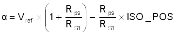
Let α = Va for simplicity, and α can be obtained from Equation 2. The voltage at junction a, which is α, is determined by ISO_POS which is measured by ADC.
When only S2 is closed, there are also two leakage current paths for the high-voltage battery. One leakage current, which goes through high-voltage battery, flows from the positive terminal of high-voltage battery (junction a) to chassis ground, and depends on the positive terminal voltage (referred to chassis ground) and RISOP. The other leakage current flows from the negative terminal of high-voltage battery (junction b) to chassis ground, and depends on the negative terminal voltage (referred to chassis ground) and RISON.
 Figure 2-2 Measurement Prodedure: Only One Switch
is Closed Periodically
Figure 2-2 Measurement Prodedure: Only One Switch
is Closed PeriodicallySimilarly, the equations of junction b and junction d can be obtained according to Kirchhoff's Current Law respectively.
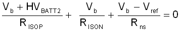
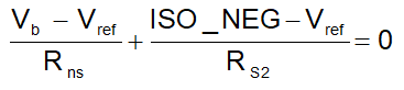
Here Vb is the voltage at junction b, which is the high-battery negative terminal voltage referred to chassis ground. Vref is the reference voltage applied to op-amp non-inverting input (+). Rns is the sum of Rns1 and Rns2, that is, Rns=Rns1+Rns2. HVBATT2 is the battery voltage measured by ADC when only S2 is closed. ISO_NEG is the bottom op-amp output voltage during the same scenario. HVBATT2 and ISO_NEG should be sampled by ADC synchronously for calculation accuracy.
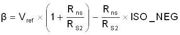
Similarly, let β = Vb for simplicity, then β can be derived from Equation 5. The voltage at junction b, which is β, can be determined by ISO_NEG which is also measured by ADC.
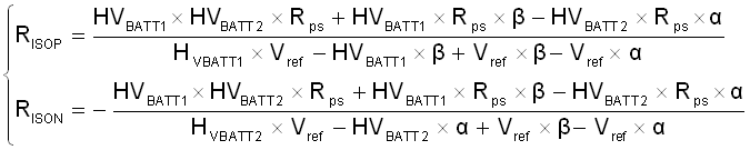
Different equations are seen during these two switching scenarios, which can be combined to calculate desired RISOP and RISON. Equation 1 and Equation 4 are combined to form an equation group while replacing Va and Vb α with and β respectively.
Let Rps equals to Rns in the design, that is, Rps = Rns, then RISOP and RISON are found from above equation group.
Generally, the value of α is positive and the value of β is negative as they are referred to chassis ground. In consequence, the ADC measured ISO_POS is smaller than Vref and ISO_NEG is larger than Vref. The absolute values of both α and β are much larger than zero under typical conditions as long as no terminal is shorted to chassis ground.
Equation 8 is the explicit formula, that can be integrated in the software to get the desired insulation resistance RISOP and RISON.