TIDT234 November 2022
3.2 Output Voltage Ripple
The following set of figures show the output voltage ripple between PFM and FPWM modes, at 30-V input at no load and 1-A load conditions.
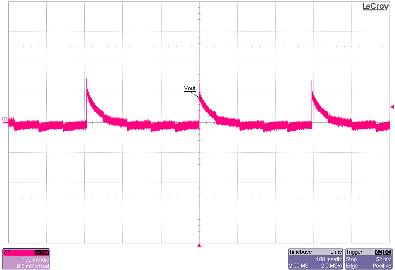 Figure 3-7 Output Voltage Ripple, No Load,
PFM-Mode
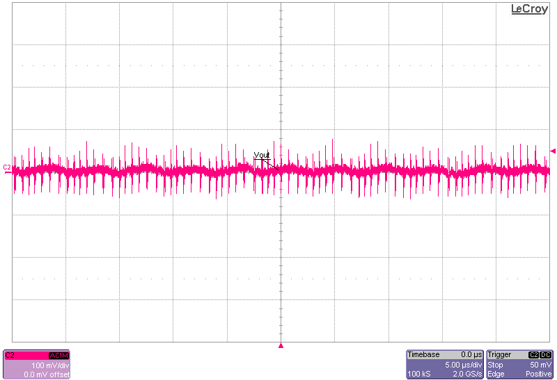 Figure 3-8 Output Voltage Ripple, No Load,
FPWM-Mode
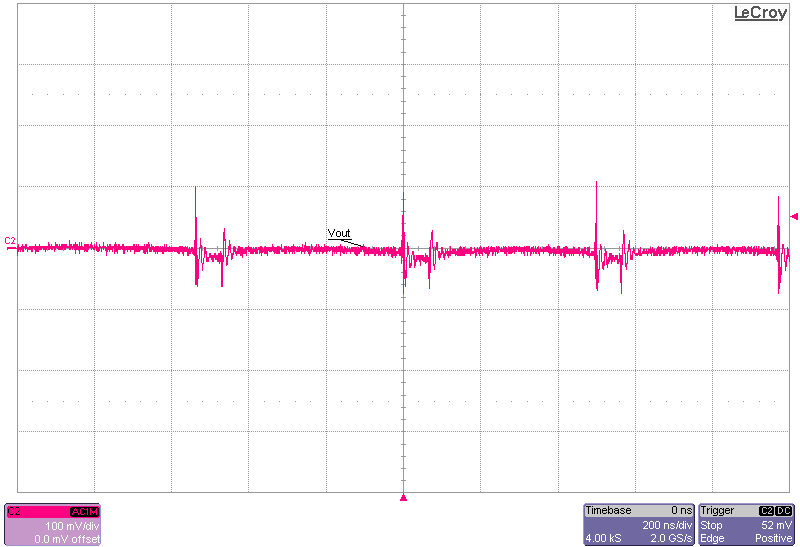 Figure 3-9 Output Voltage Ripple, 1-A Load,
PFM-Mode
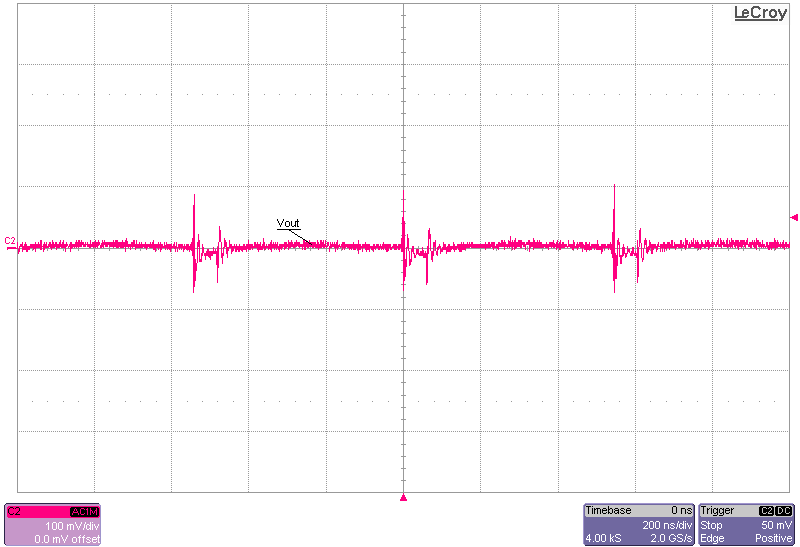 Figure 3-10 Output Voltage Ripple, 1-A Load,
FPWM-Mode
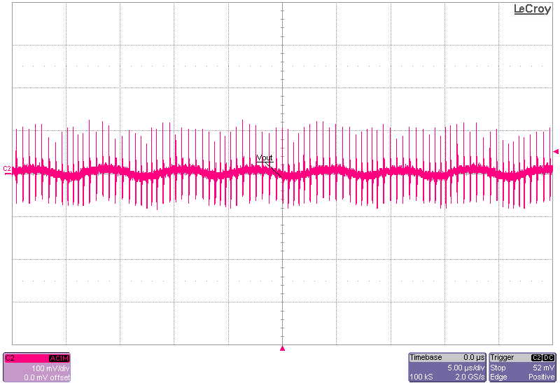 Figure 3-11 Output Voltage Ripple, 1-A Load, Zoomed Out,
PFM-Mode
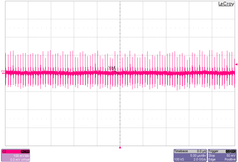 Figure 3-12 Output Voltage Ripple, 1-A Load, Zoomed Out,
FPWM-Mode