TIDT320A january 2023 – july 2023
1.1 Voltage and Current Requirements
Table 1-1 Voltage and Current
Requirements
| Parameter | Specifications |
|---|---|
| Input voltage range (Full rated power) | 250 VDC–410 VDC |
| Extended input voltage range (50% Rated power) | 100 VDC–410 VDC |
| 12VSB and S12V maximum load current (combined) | 3.7 A |
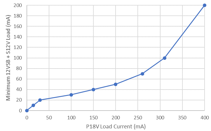
| P18V maximum load current (see Figure 1-1 for minimum load requirements on 12VSB and S12V) | 400 mA |
| Worst-case 12VSB load current mismatch between 2 paralleled units (calculated) | 30% |
 Figure 1-1 P18V Minimum Load
Requirements