TIDT382 February   2024


  1.   1
  2.   Description
  3.   Features
  4.   Applications
  5. 1Test Prerequisites
    1. 1.1 Voltage and Current Requirements
    2. 1.2 Considerations
    3. 1.3 Dimensions
  6. 2Testing and Results
    1. 2.1 Efficiency Graphs
      1. 2.1.1 LM25180-Q1 Efficiency Graph
      2. 2.1.2 SN6507-Q1 Efficiency Graph
      3. 2.1.3 UCC14130-Q1 Efficiency Graph
      4. 2.1.4 UCC25800-Q1 Efficiency Graph
      5. 2.1.5 Efficiency Comparison
    2. 2.2 Efficiency Data
      1. 2.2.1 LM25180-Q1 Efficiency Data
      2. 2.2.2 SN6507-Q1 Efficiency Data
      3. 2.2.3 UCC14130-Q1 Efficiency Data
      4. 2.2.4 UCC25800-Q1 Efficiency Data
    3. 2.3 Load Regulation
      1. 2.3.1 LM25180-Q1 Load Regulation
      2. 2.3.2 SN6507-Q1 Load Regulation
      3. 2.3.3 UCC14130-Q1 Load Regulation
      4. 2.3.4 UCC25800-Q1 Load Regulation
      5. 2.3.5 Load Regulation Comparison
    4. 2.4 Thermal Images
      1. 2.4.1 LM25180-Q1 Thermal Image
      2. 2.4.2 SN6507-Q1 Thermal Image
      3. 2.4.3 UCC14130-Q1 Thermal Image
      4. 2.4.4 UCC25800-Q1 Thermal Image
    5. 2.5 Common-Mode Current (CMI)
      1. 2.5.1 LM25180-Q1 CMI
      2. 2.5.2 SN6507-Q1 CMI
      3. 2.5.3 UCC14130-Q1 CMI
      4. 2.5.4 UCC25800-Q1 CMI
      5. 2.5.5 Common-Mode Current Comparison
  7. 3Waveforms
    1. 3.1 Switching
      1. 3.1.1 LM25180-Q1 Switching
      2. 3.1.2 SN6507-Q1 Switching
      3. 3.1.3 UCC25800-Q1 Switching
    2. 3.2 Output Voltage Ripple
      1. 3.2.1 LM25180-Q1 Output Voltage Ripple
      2. 3.2.2 SN6507-Q1 Output Voltage Ripple
      3. 3.2.3 UCC14130-Q1 Output Voltage Ripple
      4. 3.2.4 UCC25800-Q1 Output Voltage Ripple
      5. 3.2.5 Output Voltage Ripple Comparison
    3. 3.3 Input Voltage Ripple
      1. 3.3.1 LM25180-Q1 Input Voltage Ripple
      2. 3.3.2 SN6507-Q1 Input Voltage Ripple
      3. 3.3.3 UCC14130-Q1 Input Voltage Ripple
      4. 3.3.4 UCC25800-Q1 Input Voltage Ripple
      5. 3.3.5 Input Voltage Ripple Comparison
    4. 3.4 Load Transients
      1. 3.4.1 LM25180-Q1 Load Transients
      2. 3.4.2 SN6507-Q1 Load Transients
      3. 3.4.3 UCC14130-Q1 Load Transients
      4. 3.4.4 UCC25800-Q1 Load Transients
    5. 3.5 Start-Up Sequence
      1. 3.5.1 LM25180-Q1 Start-Up Sequence
      2. 3.5.2 SN6507 Q1 Start Up Sequence
      3. 3.5.3 UCC14130-Q1 Start-Up Sequence
      4. 3.5.4 UCC25800-Q1 Start-Up Sequence
    6. 3.6 Shutdown Sequence
      1. 3.6.1 LM25180-Q1 Shutdown Sequence
      2. 3.6.2 SN6507-Q1 Shutdown Sequence
      3. 3.6.3 UCC14130-Q1 Shutdown Sequence
      4. 3.6.4 UCC25800-Q1 Shutdown Sequence
    7. 3.7 Undervoltage Protection
      1. 3.7.1 LM25180-Q1 Undervoltage Protection
      2. 3.7.2 SN6507-Q1 Undervoltage Protection
      3. 3.7.3 UCC14130-Q1 Undervoltage Protection
      4. 3.7.4 UCC25800-Q1 Undervoltage Protection
  8. 4Summary
  9. 5References

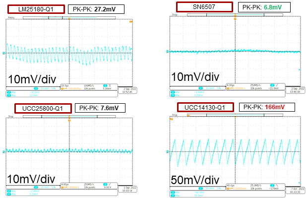
Output Voltage Ripple Comparison

The output voltage ripple comparison waveforms are shown in the following figure.
GUID-20240116-SS0I-8Z6R-PF7C-W2KZC1MQXJVW-low.png
The isolated DCDC module uses an ON-OFF control scheme that results in larger input ripple and output ripple.
Figure 3-8 Output Voltage Ripple Comparison