TIDT382 February   2024


  1.   1
  2.   Description
  3.   Features
  4.   Applications
  5. 1Test Prerequisites
    1. 1.1 Voltage and Current Requirements
    2. 1.2 Considerations
    3. 1.3 Dimensions
  6. 2Testing and Results
    1. 2.1 Efficiency Graphs
      1. 2.1.1 LM25180-Q1 Efficiency Graph
      2. 2.1.2 SN6507-Q1 Efficiency Graph
      3. 2.1.3 UCC14130-Q1 Efficiency Graph
      4. 2.1.4 UCC25800-Q1 Efficiency Graph
      5. 2.1.5 Efficiency Comparison
    2. 2.2 Efficiency Data
      1. 2.2.1 LM25180-Q1 Efficiency Data
      2. 2.2.2 SN6507-Q1 Efficiency Data
      3. 2.2.3 UCC14130-Q1 Efficiency Data
      4. 2.2.4 UCC25800-Q1 Efficiency Data
    3. 2.3 Load Regulation
      1. 2.3.1 LM25180-Q1 Load Regulation
      2. 2.3.2 SN6507-Q1 Load Regulation
      3. 2.3.3 UCC14130-Q1 Load Regulation
      4. 2.3.4 UCC25800-Q1 Load Regulation
      5. 2.3.5 Load Regulation Comparison
    4. 2.4 Thermal Images
      1. 2.4.1 LM25180-Q1 Thermal Image
      2. 2.4.2 SN6507-Q1 Thermal Image
      3. 2.4.3 UCC14130-Q1 Thermal Image
      4. 2.4.4 UCC25800-Q1 Thermal Image
    5. 2.5 Common-Mode Current (CMI)
      1. 2.5.1 LM25180-Q1 CMI
      2. 2.5.2 SN6507-Q1 CMI
      3. 2.5.3 UCC14130-Q1 CMI
      4. 2.5.4 UCC25800-Q1 CMI
      5. 2.5.5 Common-Mode Current Comparison
  7. 3Waveforms
    1. 3.1 Switching
      1. 3.1.1 LM25180-Q1 Switching
      2. 3.1.2 SN6507-Q1 Switching
      3. 3.1.3 UCC25800-Q1 Switching
    2. 3.2 Output Voltage Ripple
      1. 3.2.1 LM25180-Q1 Output Voltage Ripple
      2. 3.2.2 SN6507-Q1 Output Voltage Ripple
      3. 3.2.3 UCC14130-Q1 Output Voltage Ripple
      4. 3.2.4 UCC25800-Q1 Output Voltage Ripple
      5. 3.2.5 Output Voltage Ripple Comparison
    3. 3.3 Input Voltage Ripple
      1. 3.3.1 LM25180-Q1 Input Voltage Ripple
      2. 3.3.2 SN6507-Q1 Input Voltage Ripple
      3. 3.3.3 UCC14130-Q1 Input Voltage Ripple
      4. 3.3.4 UCC25800-Q1 Input Voltage Ripple
      5. 3.3.5 Input Voltage Ripple Comparison
    4. 3.4 Load Transients
      1. 3.4.1 LM25180-Q1 Load Transients
      2. 3.4.2 SN6507-Q1 Load Transients
      3. 3.4.3 UCC14130-Q1 Load Transients
      4. 3.4.4 UCC25800-Q1 Load Transients
    5. 3.5 Start-Up Sequence
      1. 3.5.1 LM25180-Q1 Start-Up Sequence
      2. 3.5.2 SN6507 Q1 Start Up Sequence
      3. 3.5.3 UCC14130-Q1 Start-Up Sequence
      4. 3.5.4 UCC25800-Q1 Start-Up Sequence
    6. 3.6 Shutdown Sequence
      1. 3.6.1 LM25180-Q1 Shutdown Sequence
      2. 3.6.2 SN6507-Q1 Shutdown Sequence
      3. 3.6.3 UCC14130-Q1 Shutdown Sequence
      4. 3.6.4 UCC25800-Q1 Shutdown Sequence
    7. 3.7 Undervoltage Protection
      1. 3.7.1 LM25180-Q1 Undervoltage Protection
      2. 3.7.2 SN6507-Q1 Undervoltage Protection
      3. 3.7.3 UCC14130-Q1 Undervoltage Protection
      4. 3.7.4 UCC25800-Q1 Undervoltage Protection
  8. 4Summary
  9. 5References

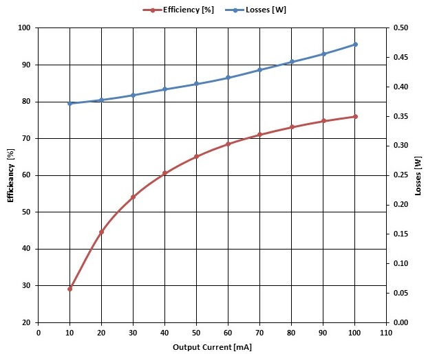
SN6507-Q1 Efficiency Graph

GUID-20240116-SS0I-VBCW-Q482-WCJJV63N9GKH-low.jpg Figure 2-2 SN6507-Q1 Efficiency at 15 VIN
Note: The efficiency graph shows only up to 100mA load current. The SN6507-Q1 device has 0.5A rated power switches. Maximum efficiency of this device can be achieved in the range of 250mA–300mA load current.