TIDUDT4A May 2018 – November 2021 AM3351 , AM3352 , AM3354 , AM3356 , AM3357 , AM3358 , AM3358-EP , AM3359
- Description
- Resources
- Features
- Applications
- 5
- 1System Description
- 2System Overview
- 3Hardware, Software, Testing Requirements, and Test Results
- 4Design Files
- 5Software Files
- 6Related Documentation
- 7About the Author
- 8Revision History
4.3.1 PCB Layout Guidelines
The board's PCB is set up for 6 layers; the 1, 3, 4, and 6 layers are signal layers, the 2 layer is a GND layer, and the 5 layer is a power layer. The PCB layers are shown in Figure 4-1 through Figure 4-6.
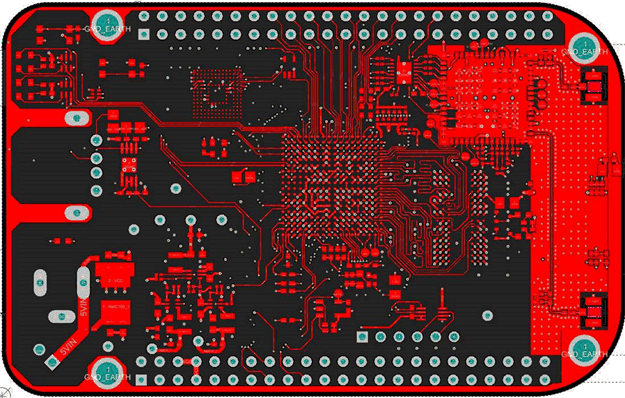 Figure 4-1 Top Layer of TIDA-01568
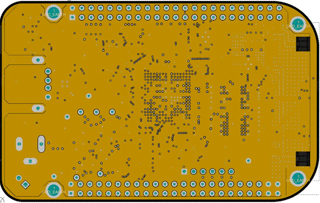 Figure 4-2 Layer 2 of TIDA-01568
 Figure 4-3 Layer 3 of TIDA-01568
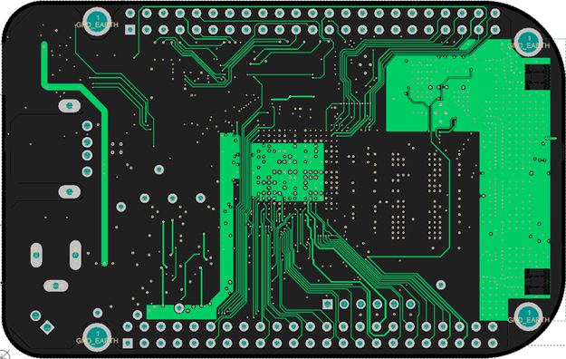 Figure 4-4 Layer 4 of TIDA-01568
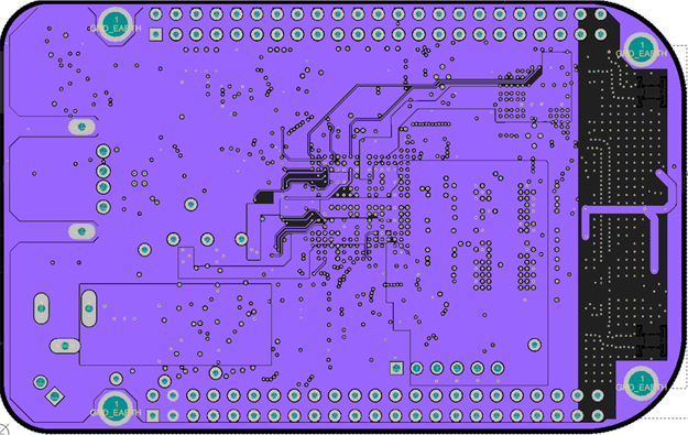 Figure 4-5 Layer 5 of TIDA-01568
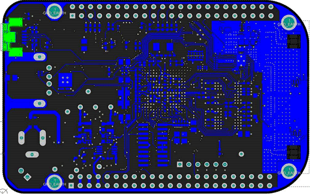 Figure 4-6 Bottom Layer of TIDA-01568
During the layout for DC-DC, coupling between different loops should be avoided. Place the input capacitor as close as possible to the device. The noise sensitive loop should be separated with high di/dt loops, so that the feedback trace should be put as far as possible from components and traces with high di/dt. Another key concern is the ground plane: it should be as large as possible to reduce noise sensitivity and improve thermal dissipation.
Another concern during layout is for the WL183xMOD: keep the proximity of ground vias close to the pad. There should be 4 vias per pad, and a complete ground pattern under the module for better thermal performance. In this design, the GND pour is added on layer 3 and layer 4 under the module.
During the layout for the antenna, use a 50-Ω impedance match on the trace to the antenna, and 50-Ω traces for the PCB layout. RF traces must have via stitching on the ground plane beside the RF trace on both sides. RF traces must have constant impedance (microstrip transmission line). RF trace bends must be gradual, with an approximate maximum bend of 45 degrees with trace mitered. RF traces must not have sharp corners. The RF trace antenna feed must be as short as possible beyond the ground reference. At this point, the trace starts to radiate.
For more details on WiLink layout, refer to the WL1837MODCOM8I WLAN MIMO and BT Module EVB for TI Sitara Platform User's Guide.