TIDUDT4A May 2018 – November 2021 AM3351 , AM3352 , AM3354 , AM3356 , AM3357 , AM3358 , AM3358-EP , AM3359
- Description
- Resources
- Features
- Applications
- 5
- 1System Description
- 2System Overview
- 3Hardware, Software, Testing Requirements, and Test Results
- 4Design Files
- 5Software Files
- 6Related Documentation
- 7About the Author
- 8Revision History
2.2.2 Power Sequencing Requirements of the System
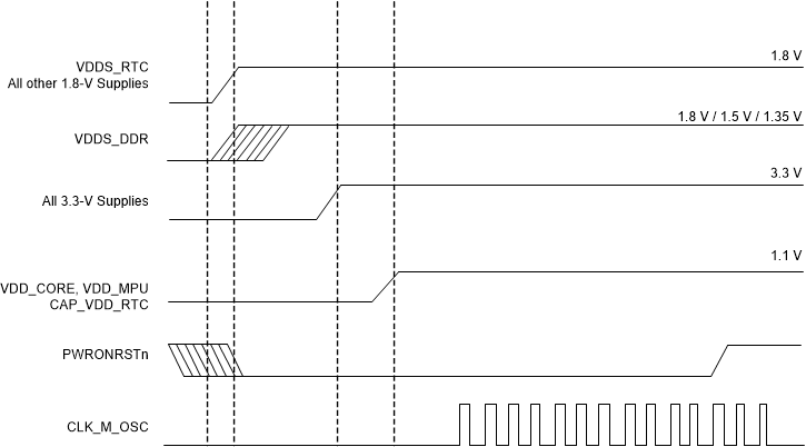
Power sequencing requirements are another key consideration. The operation mode of this system has been set as RTC Feature Disable, the details of power sequencing requirements are shown in Figure 6-6 of AM335x data sheet. In this mode, consider the configuration for each pin related to RTC functionality when designing the schematic. The use case scenarios are provided in the AM335x_Schematic_Checklist.
Figure 2-2 shows the power sequence requirements of the AM335x for this system.
 Figure 2-2 Power Supply Sequencing for AM335x with RTC Feature Disabled
The requirements for the power-up sequencing:
- VDDS_RTC and all other 1.8-V supplies ramp up.
- VDD_DDR, which has been set at 1.35 V, ramp up at second order.
- All 3.3-V supplies ramp up at third order.
- VDD_CORE at 1.1 V and VDD_MPU at 1.325 V ramp up after the 3.3-V rail goes high and at fourth order.
- PWRONRSTn ramps up after all other rails go high.
The requirements for the power-down sequencing:
- The PWRONRSTn input terminal should be taken low, which stops all internal clocks before the power supplies are turned off. All other external clocks to the device should be shut off.
- The preferred method to sequence power down is to have all the power supplies ramped down sequentially in the exact reverse order of the power-up sequencing. In other words, the power supply that was ramped up first should be the last one to be ramped down. This ensures there are no spurious current paths during the power-down sequence. The VDDS power supply must ramp down after all 3.3-V VDDSHVx [1-6] power supplies.
- If it is desired to ramp down VDDS and VDDSHVx[1-6] simultaneously, it should always be ensured that the difference between VDDS and VDDSHVx[1-6] during the entire power-down sequence is < 2 V. Any violation of this could cause reliability risks for the device. Further, TI recommends maintaining VDDS ≥ 1.5 V, as all the other supplies fully ramp down to minimize in-rush currents.
- If none of the VDDSHVx [1-6] power supplies are configured as 3.3 V, the VDDS power supply may ramp down along with the VDDSHVx [1-6] supplies, or after all the VDDSHVx [1-6] supplies have ramped down. TI recommends maintaining VDDS ≥ 1.5 V, as all the other supplies fully ramp down to minimize in-rush currents.
The VBAT and VIO for the WL183xMOD do not have a strict requirement on which can come up first. However, there are strict requirements for the Enable and Clock power sequences, which are outlined on Section 5.22.2 of the WL18x7MOD data sheet .