TIDUE53I march   2018  – july 2023 TMS320F28P550SJ , TMS320F28P559SJ-Q1


  1.   1
  2.   Description
  3.   Resources
  4.   Features
  5.   Applications
  6.   6
  7. 1System Description
    1. 1.1 Key System Specifications
  8. 2System Overview
    1. 2.1 Block Diagram
    2. 2.2 Highlighted Products
      1. 2.2.1  UCC21710
      2. 2.2.2  UCC5320
      3. 2.2.3  TMS320F28379D
      4. 2.2.4  AMC1305M05
      5. 2.2.5  OPA4340
      6. 2.2.6  LM76003
      7. 2.2.7  PTH08080W
      8. 2.2.8  TLV1117
      9. 2.2.9  OPA350
      10. 2.2.10 UCC14240
    3. 2.3 System Design Theory
      1. 2.3.1 Three-Phase T-Type Inverter
        1. 2.3.1.1 Architecture Overview
        2. 2.3.1.2 LCL Filter Design
        3. 2.3.1.3 Inductor Design
        4. 2.3.1.4 SiC MOSFETs Selection
        5. 2.3.1.5 Loss Estimations
        6. 2.3.1.6 Thermal Considerations
      2. 2.3.2 Voltage Sensing
      3. 2.3.3 Current Sensing
      4. 2.3.4 System Power Supplies
        1. 2.3.4.1 Main Input Power Conditioning
        2. 2.3.4.2 Isolated Bias Supplies
      5. 2.3.5 Gate Drivers
        1. 2.3.5.1 1200-V SiC MOSFETs
        2. 2.3.5.2 650-V SiC MOSFETs
        3. 2.3.5.3 Gate Driver Bias Supply
      6. 2.3.6 Control Design
        1. 2.3.6.1 Current Loop Design
        2. 2.3.6.2 PFC DC Bus Voltage Regulation Loop Design
  9. 3Hardware, Software, Testing Requirements, and Test Results
    1. 3.1 Required Hardware and Software
      1. 3.1.1 Hardware
        1. 3.1.1.1 Test Hardware Required
        2. 3.1.1.2 Microcontroller Resources Used on the Design (TMS320F28379D)
        3. 3.1.1.3 F28377D, F28379D Control-Card Settings
        4. 3.1.1.4 Microcontroller Resources Used on the Design (TMS320F280039C)
      2. 3.1.2 Software
        1. 3.1.2.1 Getting Started With Firmware
          1. 3.1.2.1.1 Opening the CCS project
          2. 3.1.2.1.2 Digital Power SDK Software Architecture
          3. 3.1.2.1.3 Interrupts and Lab Structure
          4. 3.1.2.1.4 Building, Loading and Debugging the Firmware
        2. 3.1.2.2 Protection Scheme
        3. 3.1.2.3 PWM Switching Scheme
        4. 3.1.2.4 ADC Loading
    2. 3.2 Testing and Results
      1. 3.2.1 Lab 1
      2. 3.2.2 Testing Inverter Operation
        1. 3.2.2.1 Lab 2
        2. 3.2.2.2 Lab 3
        3. 3.2.2.3 Lab 4
      3. 3.2.3 Testing PFC Operation
        1. 3.2.3.1 Lab 5
        2. 3.2.3.2 Lab 6
        3. 3.2.3.3 Lab 7
      4. 3.2.4 Test Setup for Efficiency
      5. 3.2.5 Test Results
        1. 3.2.5.1 PFC Mode - 230 VRMS, 400 V L-L
          1. 3.2.5.1.1 PFC Start-up – 230 VRMS, 400 L-L AC Voltage
          2. 3.2.5.1.2 Steady State Results at 230 VRMS, 400 V L-L - PFC Mode
          3. 3.2.5.1.3 Efficiency and THD Results at 220 VRMS, 50 Hz – PFC Mode
          4. 3.2.5.1.4 Transient Test With Step Load Change
        2. 3.2.5.2 PFC Mode - 120 VRMS, 208 V L-L
          1. 3.2.5.2.1 Steady State Results at 120 VRMS, 208 V-L-L - PFC Mode
          2. 3.2.5.2.2 Efficiency and THD Results at 120 VRMS - PFC Mode
        3. 3.2.5.3 Inverter Mode
          1. 3.2.5.3.1 Inverter Closed Loop Results
          2. 3.2.5.3.2 Efficiency and THD Results - Inverter Mode
          3. 3.2.5.3.3 Inverter - Transient Test
      6. 3.2.6 Open Loop Inverter Test Results
  10. 4Design Files
    1. 4.1 Schematics
    2. 4.2 Bill of Materials
    3. 4.3 PCB Layout Recommendations
      1. 4.3.1 Layout Prints
    4. 4.4 Altium Project
    5. 4.5 Gerber Files
    6. 4.6 Assembly Drawings
  11. 5Trademarks
  12. 6About the Authors
  13. 7Revision History

UCC5320

The UCC53x0 is a family of compact, single-channel, isolated IGBT, SiC, and MOSFET gate drivers with best-in-class isolation ratings and variants for pinout configuration, and drive strength.

The UCC53x0 is available in an 8-pin SOIC (DWV) package. This package has a creepage and clearance of 8.5 mm and can support isolation voltage up to 5 kVRMS, which is good for applications where reinforced isolation is needed. With these various options and wide power range, the UCC53x0 family is a good fit for motor drives and industrial power supplies.

  • 3-V to 15-V input supply voltage
  • 13.2-V to 33-V output driver supply voltage
  • Feature options:
    • Split outputs (UCC5320S and UCC5390S)
    • UVLO with respect to MOSFET collector (UCC5320E and UCC5390E)
    • Miller clamp option (UCC5310M and UCC5350M)
  • Negative 5-V handling capability on input pins
  • 60-ns (typical) propagation delay for UCC5320S, UCC5320E, and UCC5310M
  • 100-kV/µs minimum CMTI
  • Isolation surge withstand voltage: 4242 VPK
  • Safety-related certifications:
    • 4242-VPK isolation per DIN V VDE V 0884-10 and DIN EN 61010-1 (planned)
    • 3000-VRMS isolation for 1 minute per UL 1577 (planned)
    • CSA Component Acceptance Notice 5A, IEC 60950-1 and IEC 61010-1 End Equipment Standards (Planned)
    • CQC Certification per GB4943.1-2011 (Planned)
  • 4-kV ESD on all pins
  • CMOS inputs
  • 8-pin narrow body SOIC package
  • Operating temperature: –40°C to +125°C ambient
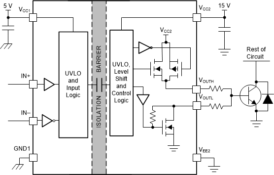
GUID-53F1F637-F31F-4CD6-8097-2F87EA4B98E3-low.gifFigure 2-3 UCC5320 Functional Block Diagram (S Version)