TIDUE53I march 2018 – july 2023 TMS320F28P550SJ , TMS320F28P559SJ-Q1
- 1
- Description
- Resources
- Features
- Applications
- 6
- 1System Description
- 2System Overview
-
3Hardware, Software, Testing Requirements, and Test Results
- 3.1 Required Hardware and Software
- 3.2 Testing and Results
- 4Design Files
- 5Trademarks
- 6About the Authors
- 7Revision History
2.3.6 Control Design
Terminology:
-
Vbus or Vdc
bus voltage for the inverter
-
Li and Ri
inductance of the inverter side inductor and series resistance
-
Lg and Rg
inductance of the grid side inductor, and series resistance
-
Cf and Rf
capacitance value and series resistor plus any damping resistor
-
vi_a,vi_b,vi_c
output voltage from the three phase bridge, this voltage is what is
controlled using the duty cycle control of the three phase bridge
Therefore, for control purposes it is assumed now only the modulation needs to change between 2-level and 3-level inverter for the power stage and control design can remain the same. Where ,Da, Db, Dc, are the control variable generated such that the output voltage of the inverter can be represented as Equation 49:
Equation 34. 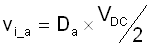
-
ii_a, ii_b, ii_c
current through the inverter side inductor
-
vx_a, vx_b, vx_c
voltage across the filter capacitor
-
ig_a, ig_b, ig_c
voltage across the filter capacitor
-
vg_a, vg_b, vg_c
grid frequency