SLOA278 July 2021 OPA4325 , TLV9052 , TLV9064
Design Goals
| AC Specifications | Supply | ||
|---|---|---|---|
| AC Gain | foscillation | Vcc | Vee |
| 8V/V | 10kHz | 2.5V | –2.5V |
Design Description
This circuit uses a quad channel op amp with ±2.5-V supplies to generate a 10kHz, low-distortion sine wave. The amplifiers buffer each RC filter stage, which yields a low-distortion output.
Design Notes
- Using excessively large feedback resistors, R1 and R2, can lead to a shift in oscillation frequency, and an increase in noise and distortion.
- The first stage resistors, R1 and R2, must be selected to provide a sufficiently large gain. Otherwise, oscillations at the output will dampen. However, an excessively large gain at the first stage will lead to higher output distortion and a decreased frequency of oscillation.
- Heavy loading of the output leads to degradation in the oscillation frequency.
- At higher frequencies (> 10 kHz), the phase delay of the amplifier becomes significant. The result will be a frequency of oscillation that is lower than calculated or expected. Thus, some margin must be included when selecting values for the loading elements of the first, second, and third stages (R3, R4, R5, C1, C2, and C3) for higher-frequency designs to ensure the desired oscillation frequency is achieved.
- Choose an amplifier with at least 100 times the required gain bandwidth product. This will ensure the actual and calculated oscillation frequencies match.
- For more precise control of the oscillation frequency, use passive components with lower tolerances.
Design Steps
For a classical feedback system, oscillation occurs when the product of the open loop gain, AOL, and the feedback factor, β, is equal to –1, or 1 at 180°. Therefore, each RC stage in the design must contribute 60° of phase shift. Since each stage is isolated by a buffer, the feedback factor, β, of the first stage must have a magnitude of (1/2)3. Therefore the gain (1/β) must be at least 8V/V.
- Select the first stage feedback resistors for the gain necessary to maintain oscillation.
- Calculate components R3,
R4, R5, C1, C2, and
C3 to set the oscillation frequency. Select C1,
C2, and C3 as 10nF.
- Ensure the selected op amp has the
bandwidth to oscillate at the desired frequency.
- Ensure the selected op amp has the
slew rate necessary to oscillate at the desired frequency. Use the full power
bandwidth equation to calculate the necessary slew rate and ensure it is less
than the slew rate of the amplifier. While the exact amplitude of oscillation is
difficult to predict, you can ensure that our amplifier is fast enough to
generate the needed sine wave by ensuring that the output can swing from
rail-to-rail.
Design Simulations
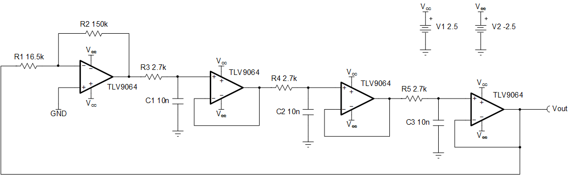
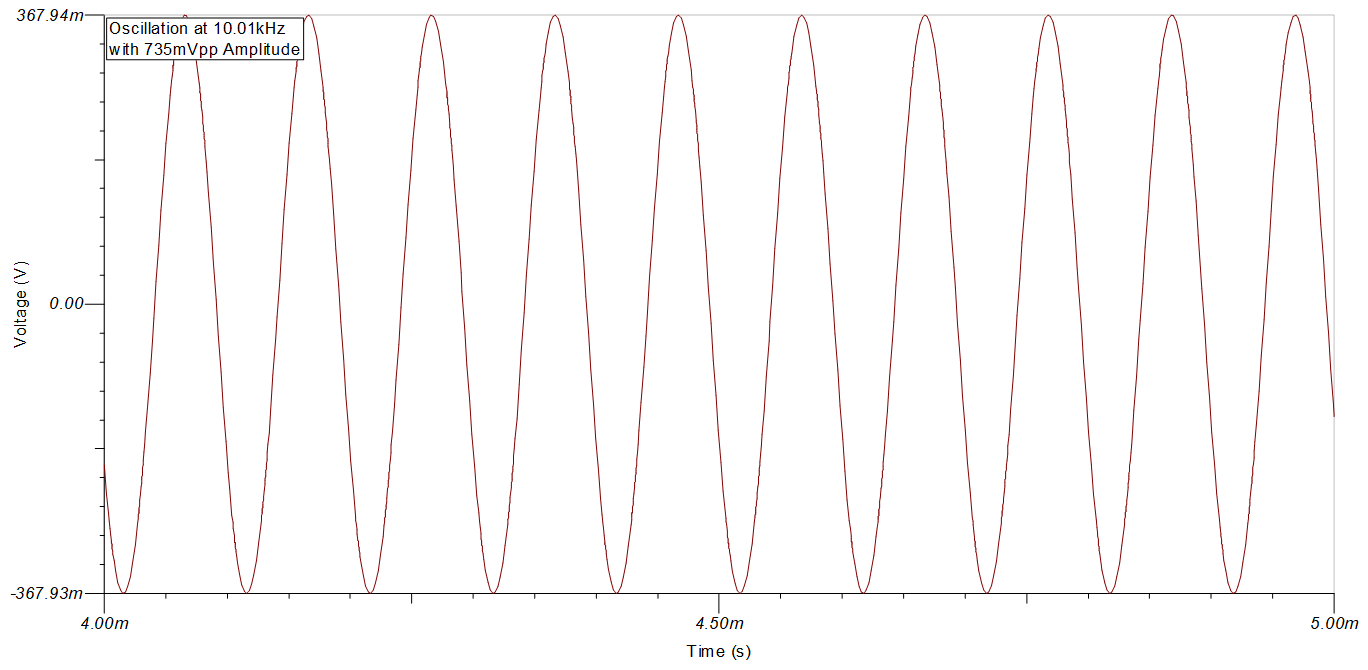
The resulting simulations demonstrate a sinusoidal oscillator that reaches steady state after about 3ms to a 10.01-kHz sine wave with a 735-mVpp amplitude.
Transient Simulation Results
Design References
- See Analog Engineer's Circuit Cookbooks for TI's comprehensive circuit library.
- SPICE Simulation File: SLOC355.
- TI Precision Labs
- Sine-Wave Oscillator Application Report
- Design of Op Amp Sine Wave Generators Application Report
Design Featured Op Amp
| TLV9064 | |
|---|---|
| Vss | 1.8V to 5.5V |
| VinCM | Rail-to-rail |
| Vout | Rail-to-rail |
| Vos | 300µV |
| Iq | 538µA |
| Ib | 0.5pA |
| UGBW | 10MHz |
| SR | 6.5V/µs |
| #Channels | 1, 2, 4 |
| www.ti.com/product/TLV9064 | |
Design Alternate Op Amps
| TLV9052 | OPA4325 | |
|---|---|---|
| Vss | 1.8V to 5.5V | 2.2V to 5.5V |
| VinCM | Rail–to–rail | Rail–to–rail |
| Vout | Rail–to–rail | Rail–to–rail |
| Vos | 330µV | 40µV |
| Iq | 330µA | 650µA |
| Ib | 2pA | 0.2pA |
| UGBW | 5MHz | 10MHz |
| SR | 15V/µs | 5V/µs |
| #Channels | 2 | 4 |
| www.ti.com/product/TLV9052 | www.ti.com/product/OPA4325 |