SBAA528 February 2022 ADC12QJ1600-Q1 , TPS62912 , TPS62913
2.3 Test Results
Performance tables and graphs comparing the original ADC12QJ1600-Q1 Original EVM with TPS62913 spread spectrum on and off modified board are shown below.
| Frequency (MHz) | Original QJ EVM (dBFS) | TPS62913 W/O SS (dBFS) | TPS62913 W/ SS (dBFS) |
|---|---|---|---|
| 97 | 57.473 | 57.35 | 57.4 |
| 397 | 57.171 | 57.14 | 57.08 |
| 597 | 56.814 | 56.66 | 56.7 |
| 797 | 56.501 | 56.36 | 56.4 |
| 997 | 55.967 | 55.98 | 55.977 |
| 1497 | 54.765 | 55.02 | 55.01 |
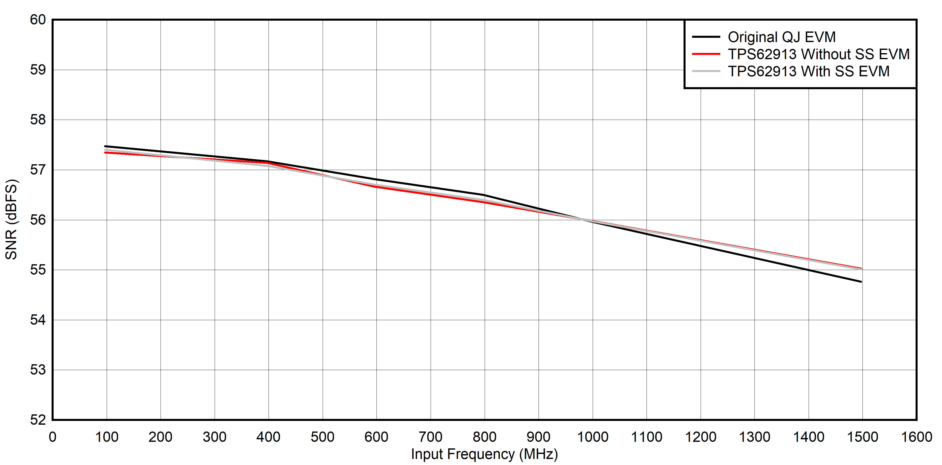 Figure 2-5 Signal to Noise (SNR)
Comparison Graph
Figure 2-5 Signal to Noise (SNR)
Comparison Graph| Frequency (Hz) | Original QJ EVM (dBFS) | TPS62913 W/O SS (dBFS) | TPS62913 W/ SS (dBFS) |
|---|---|---|---|
| 97 | 67.92 | 67.41 | 67.28 |
| 397 | 70.799 | 70.91 | 69.95 |
| 597 | 64.663 | 65.57 | 65.6 |
| 797 | 65.847 | 65.42 | 65.51 |
| 997 | 64.302 | 64.14 | 64.2 |
| 1497 | 63.485 | 63.46 | 63.4 |
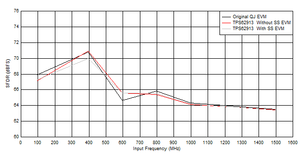 Figure 2-6 Spurious-Free Dynamic Range
Comparison Graph
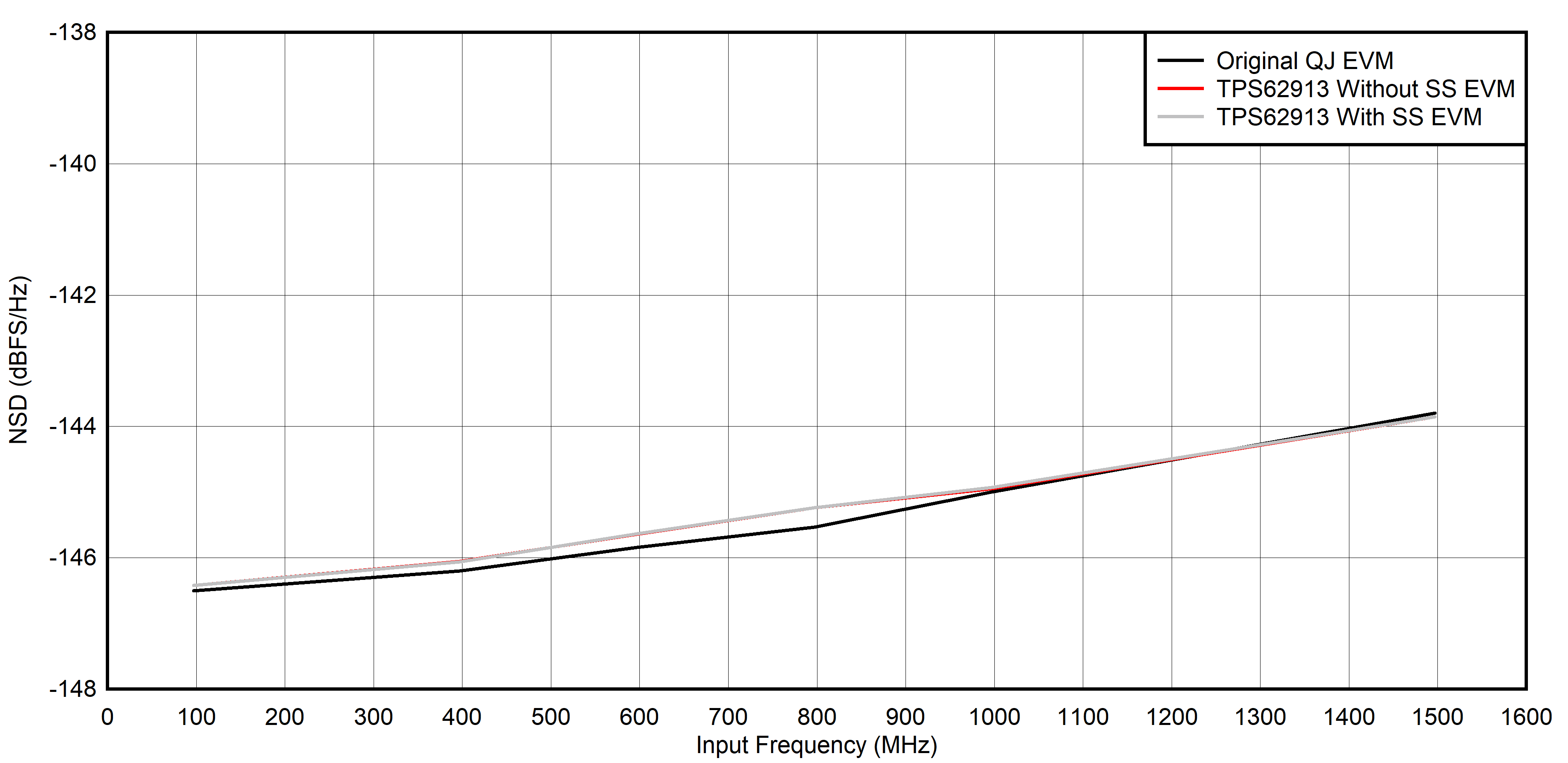 Figure 2-7 Noise Spectral Density
Comparison Graph
Figure 2-7 Noise Spectral Density
Comparison GraphThe next plot, Figure 2-8, shows how no PSMR is observed with an analog input signal frequency of 347 MHz applied when using the original power design with SMPS and LDO, and the TPS62913 switching supply with and without spread sprectrum enabled.
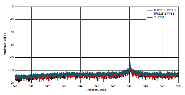 Figure 2-8 PSMR Comparison of Original
and TPS62913
Figure 2-8 PSMR Comparison of Original
and TPS62913Additionally, no visible modulation of the switcher power supply spur is seen around the carrier and at DC as seen in Figure 2-9.
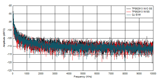 Figure 2-9 PSMR Comparison of Original
and TPS62913 at DC
Figure 2-9 PSMR Comparison of Original
and TPS62913 at DC| Configuration | Input Current | Input Power |
|---|---|---|
| Original Power Supply Configuration with SMPSs + LDOs | 486 mA | 5.832 W |
| TPS62913 Power Supplies only-UPDATE | 327 mA | 3.924 W |
| Input Current and Power Savings-UPDATE | 159 mA | 1.908W |
Figure 2-10 through Figure 2-12 are thermal images of the power supplies running when taking data for the performance comparison tables.

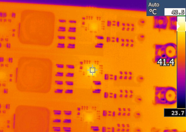
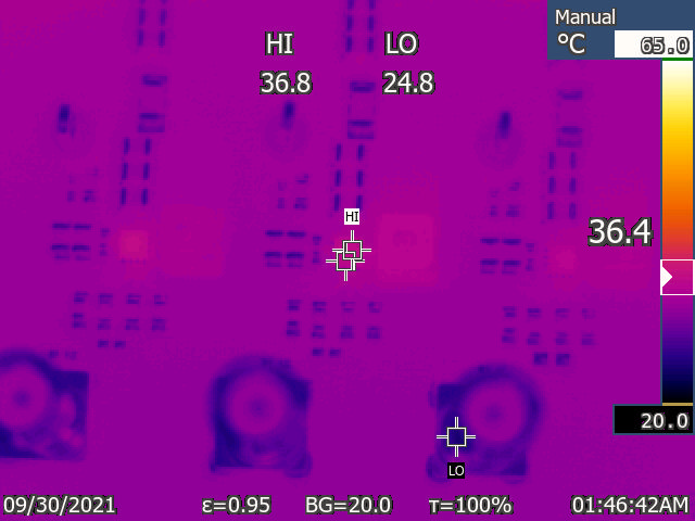 Figure 2-12 TPS62913 Switching
Converters