SBAS824 October   2018 ADS1235

PRODUCTION DATA.  

  1. Features
  2. Applications
  3. Description
    1.     Device Images
      1.      Block Diagram
      2.      ADC Conversion Noise
  4. Revision History
  5. Pin Configuration and Functions
    1.     Pin Functions
  6. Specifications
    1. 6.1 Absolute Maximum Ratings
    2. 6.2 ESD Ratings
    3. 6.3 Recommended Operating Conditions
    4. 6.4 Thermal Information
    5. 6.5 Electrical Characteristics
    6. 6.6 Timing Requirements
    7. 6.7 Switching Characteristics
    8. 6.8 Typical Characteristics
  7. Parameter Measurement Information
    1. 7.1 Noise Performance
  8. Detailed Description
    1. 8.1 Overview
    2. 8.2 Functional Block Diagram
    3. 8.3 Feature Description
      1. 8.3.1 Analog Inputs
        1. 8.3.1.1 ESD Diodes
        2. 8.3.1.2 Input Multiplexer
        3. 8.3.1.3 Temperature Sensor
        4. 8.3.1.4 Inputs Open
        5. 8.3.1.5 Internal VCOM Connection
        6. 8.3.1.6 Alternate Functions
      2. 8.3.2 PGA
        1. 8.3.2.1 Input Voltage Range
        2. 8.3.2.2 PGA Bypass Mode
      3. 8.3.3 PGA Voltage Monitor
      4. 8.3.4 Reference Voltage
        1. 8.3.4.1 External Reference
        2. 8.3.4.2 AVDD – AVSS Reference (Default)
        3. 8.3.4.3 Reference Monitor
      5. 8.3.5 General-Purpose Input/Outputs (GPIOs)
      6. 8.3.6 Modulator
      7. 8.3.7 Digital Filter
        1. 8.3.7.1 Sinc Filter
          1. 8.3.7.1.1 Sinc Filter Frequency Response
        2. 8.3.7.2 FIR Filter
          1. 8.3.7.2.1 FIR Filter Frequency Response
        3. 8.3.7.3 Filter Bandwidth
        4. 8.3.7.4 50-Hz and 60-Hz Normal Mode Rejection
    4. 8.4 Device Functional Modes
      1. 8.4.1 Conversion Control
        1. 8.4.1.1 Continuous-Conversion Mode
        2. 8.4.1.2 Pulse-Conversion Mode
        3. 8.4.1.3 Conversion Latency
        4. 8.4.1.4 Start-Conversion Delay
      2. 8.4.2 Chop Mode
      3. 8.4.3 AC-Bridge Excitation Mode
      4. 8.4.4 ADC Clock Mode
      5. 8.4.5 Power-Down Mode
        1. 8.4.5.1 Hardware Power-Down
        2. 8.4.5.2 Software Power-Down
      6. 8.4.6 Reset
        1. 8.4.6.1 Power-on Reset
        2. 8.4.6.2 Reset by Pin
        3. 8.4.6.3 Reset by Command
      7. 8.4.7 Calibration
        1. 8.4.7.1 Offset and Full-Scale Calibration
          1. 8.4.7.1.1 Offset Calibration Registers
          2. 8.4.7.1.2 Full-Scale Calibration Registers
        2. 8.4.7.2 Offset Self-Calibration (SFOCAL)
        3. 8.4.7.3 Offset System-Calibration (SYOCAL)
        4. 8.4.7.4 Full-Scale Calibration (GANCAL)
        5. 8.4.7.5 Calibration Command Procedure
        6. 8.4.7.6 User Calibration Procedure
    5. 8.5 Programming
      1. 8.5.1 Serial Interface
        1. 8.5.1.1 Chip Select (CS)
        2. 8.5.1.2 Serial Clock (SCLK)
        3. 8.5.1.3 Data Input (DIN)
        4. 8.5.1.4 Data Output/Data Ready (DOUT/DRDY)
        5. 8.5.1.5 Serial Interface Auto-Reset
      2. 8.5.2 Data Ready (DRDY)
        1. 8.5.2.1 DRDY in Continuous-Conversion Mode
        2. 8.5.2.2 DRDY in Pulse-Conversion Mode
        3. 8.5.2.3 Data Ready by Software Polling
      3. 8.5.3 Conversion Data
        1. 8.5.3.1 Status byte (STATUS)
        2. 8.5.3.2 Conversion Data Format
      4. 8.5.4 CRC
      5. 8.5.5 Commands
        1. 8.5.5.1  NOP Command
        2. 8.5.5.2  RESET Command
        3. 8.5.5.3  START Command
        4. 8.5.5.4  STOP Command
        5. 8.5.5.5  RDATA Command
        6. 8.5.5.6  SYOCAL Command
        7. 8.5.5.7  GANCAL Command
        8. 8.5.5.8  SFOCAL Command
        9. 8.5.5.9  RREG Command
        10. 8.5.5.10 WREG Command
        11. 8.5.5.11 LOCK Command
        12. 8.5.5.12 UNLOCK Command
    6. 8.6 Register Map
      1. 8.6.1  Device Identification (ID) Register (address = 00h) [reset = Cxh]
        1. Table 28. ID Register Field Descriptions
      2. 8.6.2  Device Status (STATUS) Register (address = 01h) [reset = 01h]
        1. Table 29. STATUS Register Field Descriptions
      3. 8.6.3  Mode 0 (MODE0) Register (address = 02h) [reset = 24h]
        1. Table 30. MODE0 Register Field Descriptions
      4. 8.6.4  Mode 1 (MODE1) Register (address = 03h) [reset = 01h]
        1. Table 31. MODE1 Register Field Descriptions
      5. 8.6.5  Mode 2 (MODE2) Register (address = 04h) [reset = 00h]
        1. Table 32. MODE2 Register Field Descriptions
      6. 8.6.6  Mode 3 (MODE3) Register (address = 05h) [reset = 00h]
        1. Table 33. MODE3 Register Field Descriptions
      7. 8.6.7  Reference Configuration (REF) Register (address = 06h) [reset = 05h]
        1. Table 34. REF Register Field Descriptions
      8. 8.6.8  Offset Calibration (OFCALx) Registers (address = 07h, 08h, 09h) [reset = 00h, 00h, 00h]
        1. Table 35. OFCAL0, OFCAL1, OFCAL2 Registers Field Description
      9. 8.6.9  Full-Scale Calibration (FSCALx) Registers (address = 0Ah, 0Bh, 0Ch) [reset = 00h, 00h, 40h]
        1. Table 36. FSCAL0, FSCAL1, FSCAL2 Registers Field Description
      10. 8.6.10 Reserved (RESERVED) Register (address = 0Dh) [reset = FFh]
        1. Table 37. RESERVED Register Field Descriptions
      11. 8.6.11 Reserved (RESERVED) Register (address = 0Eh) [reset = 00h]
        1. Table 38. RESERVED Register Field Descriptions
      12. 8.6.12 Reserved (RESERVED) Register (address = 0Fh) [reset = 00h]
        1. Table 39. RESERVED Register Field Descriptions
      13. 8.6.13 PGA Configuration (PGA) Register (address = 10h) [reset = 00h]
        1. Table 40. PGA Register Field Descriptions
      14. 8.6.14 Input Multiplexer (INPMUX) Register (address = 11h) [reset = FFh]
        1. Table 41. INPMUX Register Field Descriptions
  9. Application and Implementation
    1. 9.1 Application Information
      1. 9.1.1 Input Range
      2. 9.1.2 Input Overload
      3. 9.1.3 Unused Inputs and Outputs
      4. 9.1.4 Multiplexed 2-Bridge Input Example
      5. 9.1.5 AC-Bridge Excitation Example
      6. 9.1.6 Serial Interface and Digital Connections
    2. 9.2 Typical Application
      1. 9.2.1 Design Requirements
      2. 9.2.2 Detailed Design Procedure
      3. 9.2.3 Application Curves
    3. 9.3 Initialization Setup
  10. 10Power Supply Recommendations
    1. 10.1 Power-Supply Decoupling
    2. 10.2 Analog Power-Supply Clamp
    3. 10.3 Power-Supply Sequencing
  11. 11Layout
    1. 11.1 Layout Guidelines
    2. 11.2 Layout Example
  12. 12Device and Documentation Support
    1. 12.1 Documentation Support
      1. 12.1.1 Related Documentation
    2. 12.2 Receiving Notification of Documentation Updates
    3. 12.3 Community Resources
    4. 12.4 Trademarks
    5. 12.5 Electrostatic Discharge Caution
    6. 12.6 Glossary
  13. 13Mechanical, Packaging, and Orderable Information

Mechanical, Packaging, and Orderable Information

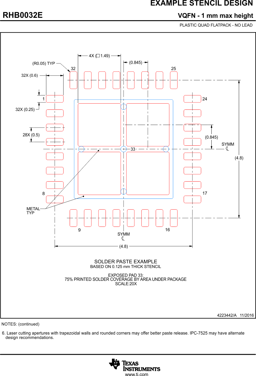
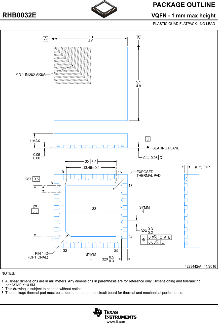
The following pages include mechanical packaging and orderable information. This information is the most current data available for the designated devices. This data is subject to change without notice and revision of this document. For browser-based versions of this data sheet, refer to the left-hand navigation.
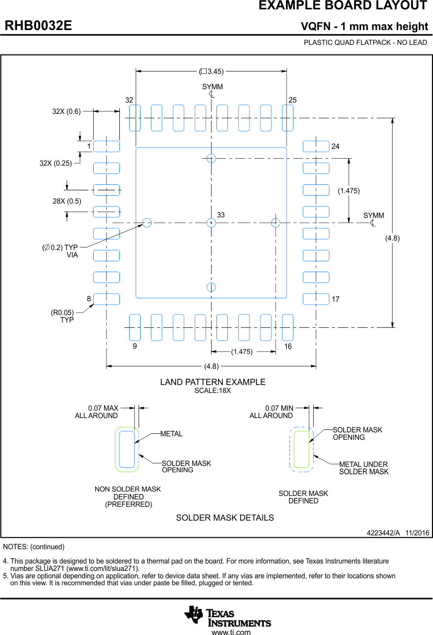
ADS1235 RHB0032E_4223442_Page_01.gif
ADS1235 RHB0032E_4223442_Page_02.gif
ADS1235 RHB0032E_4223442_Page_03.gif