SBAS891B November   2017  – September 2022 ADS7142-Q1

PRODUCTION DATA  

  1. Features
  2. Applications
  3. Description
  4. Revision History
  5. Pin Configuration and Functions
  6. Specifications
    1. 6.1  Absolute Maximum Ratings
    2. 6.2  ESD Ratings
    3. 6.3  Recommended Operating Conditions
    4. 6.4  Thermal Information
    5. 6.5  Electrical Characteristics: All Modes
    6. 6.6  Electrical Characteristics: Manual Mode
    7. 6.7  Electrical Characteristics: Autonomous Modes
    8. 6.8  Electrical Characteristics: High Precision Mode
    9. 6.9  Timing Requirements
    10. 6.10 Switching Characteristics
    11. 6.11 Timing Diagrams
    12. 6.12 Typical Characteristics: All Modes
    13. 6.13 Typical Characteristics: Manual Mode
    14. 6.14 Typical Characteristics: Autonomous Modes
    15. 6.15 Typical Characteristics: High-Precision Mode
  7. Detailed Description
    1. 7.1 Overview
    2. 7.2 Functional Block Diagram
    3. 7.3 Feature Description
      1. 7.3.1  Analog Input and Multiplexer
        1. 7.3.1.1 Two-Channel, Single-Ended Configuration
        2. 7.3.1.2 Single-Channel, Single-Ended Configuration With Remote Ground Sense
        3. 7.3.1.3 Single-Channel, Pseudo-Differential Configuration
      2. 7.3.2  Offset Calibration
      3. 7.3.3  Reference
      4. 7.3.4  ADC Transfer Function
      5. 7.3.5  Oscillator and Timing Control
      6. 7.3.6  I2C Address Selector
      7. 7.3.7  Data Buffer
        1. 7.3.7.1 Filling of the Data Buffer
        2. 7.3.7.2 Reading Data From the Data Buffer
      8. 7.3.8  Accumulator
      9. 7.3.9  Digital Window Comparator
      10. 7.3.10 I2C Protocol Features
        1. 7.3.10.1 General Call
        2. 7.3.10.2 General Call With Software Reset
        3. 7.3.10.3 General Call With Write Software Programmable Part of the Target Address
        4. 7.3.10.4 Configuring the ADC Into High-Speed I2C Mode
        5. 7.3.10.5 Bus Clear
    4. 7.4 Device Functional Modes
      1. 7.4.1 Device Power Up and Reset
      2. 7.4.2 Manual Mode
        1. 7.4.2.1 Manual Mode With CH0 Only
        2. 7.4.2.2 Manual Mode With AUTO Sequence
      3. 7.4.3 Autonomous Modes
        1. 7.4.3.1 Autonomous Mode With Threshold Monitoring and Diagnostics
          1. 7.4.3.1.1 Autonomous Mode With Pre-ALERT Data
          2. 7.4.3.1.2 Autonomous Mode With Post-ALERT Data
        2. 7.4.3.2 Autonomous Mode With Burst Data
          1. 7.4.3.2.1 Autonomous Mode With Start Burst
          2. 7.4.3.2.2 Autonomous Mode With Stop Burst
      4. 7.4.4 High-Precision Mode
    5. 7.5 Programming
      1. 7.5.1 Reading Registers
        1. 7.5.1.1 Single Register Read
        2. 7.5.1.2 Reading a Continuous Block of Registers
      2. 7.5.2 Writing Registers
        1. 7.5.2.1 Single Register Write
        2. 7.5.2.2 Writing a Continuous Block of Registers
        3. 7.5.2.3 Set Bit
        4. 7.5.2.4 Clear Bit
    6. 7.6 Register Map
      1. 7.6.1 Page1 Registers
  8. Application and Implementation
    1. 8.1 Application Information
    2. 8.2 Typical Applications
      1. 8.2.1 ADS7142-Q1 as a Programmable Comparator With False Trigger Prevention and Diagnostics
        1. 8.2.1.1 Design Requirements
        2. 8.2.1.2 Detailed Design Procedure
          1. 8.2.1.2.1 Programmable Thresholds and Hysteresis
          2. 8.2.1.2.2 False Trigger Prevention With an Event Counter
          3. 8.2.1.2.3 Fault Diagnostics With the Data Buffer
        3. 8.2.1.3 Application Curves
      2. 8.2.2 Voltage and Temperature Monitoring in Remote Camera Modules Using the ADS7142-Q1
        1. 8.2.2.1 Design Requirements
    3. 8.3 Power Supply Recommendations
      1. 8.3.1 AVDD and DVDD Supply Recommendations
    4. 8.4 Layout
      1. 8.4.1 Layout Guidelines
      2. 8.4.2 Layout Example
  9. Device and Documentation Support
    1. 9.1 Electrostatic Discharge Caution
    2. 9.2 Glossary
    3. 9.3 Trademarks
    4. 9.4 Receiving Notification of Documentation Updates
    5. 9.5 Support Resources
  10. 10Mechanical, Packaging, and Orderable Information

Oscillator and Timing Control

The device uses one of the two internal oscillators (low-power oscillator or high-speed oscillator) for converting the analog input voltage into a digital output code.

The steps for selecting the oscillator and setting the sampling speed are:

  1. Select the low-power oscillator (OSC_SEL = 1b) to monitor slow-moving signals (< 300 Hz) at extremely low-power consumption and sampling speeds (< 600 SPS). Select the high-speed oscillator (OSC_SEL = 0b) to scan the sensor signals with faster sampling speed (> 50 kHz).
  2. Set the sampling speed by programming the NCLK_SEL register:

Equation 2. GUID-D3A2B243-71C1-4278-AC75-115CC8396CD3-low.gif
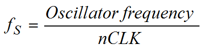
  • fs = Sampling speed.
  • Oscillator frequency = 1 / tHSO or 1 / tLPO depending on the OSC_SEL bit; see the Section 6 section for 1 / tHSO or 1 / tLPO.
  • nCLK is the number of clocks in one conversion cycle (see the NCLK_SEL register).