SBAS891B November 2017 – September 2022 ADS7142-Q1
PRODUCTION DATA
- 1 Features
- 2 Applications
- 3 Description
- 4 Revision History
- 5 Pin Configuration and Functions
-
6 Specifications
- 6.1 Absolute Maximum Ratings
- 6.2 ESD Ratings
- 6.3 Recommended Operating Conditions
- 6.4 Thermal Information
- 6.5 Electrical Characteristics: All Modes
- 6.6 Electrical Characteristics: Manual Mode
- 6.7 Electrical Characteristics: Autonomous Modes
- 6.8 Electrical Characteristics: High Precision Mode
- 6.9 Timing Requirements
- 6.10 Switching Characteristics
- 6.11 Timing Diagrams
- 6.12 Typical Characteristics: All Modes
- 6.13 Typical Characteristics: Manual Mode
- 6.14 Typical Characteristics: Autonomous Modes
- 6.15 Typical Characteristics: High-Precision Mode
-
7 Detailed Description
- 7.1 Overview
- 7.2 Functional Block Diagram
- 7.3 Feature Description
- 7.4 Device Functional Modes
- 7.5 Programming
- 7.6 Register Map
- 8 Application and Implementation
- 9 Device and Documentation Support
- 10Mechanical, Packaging, and Orderable Information
8.2.1.1 Design Requirements
In many automotive sensor monitors, a decision must be made at the system-level when the input signal crosses a predefined threshold. Analog window comparators are used extensively in such applications.
An analog window comparator has a set of comparators. The external input signal is connected to the inverting terminal of one comparator and the noninverting terminal of the other comparator. The remaining input of each comparator is connected to the internal reference. The outputs are tied together and are often connected to a reset or general-purpose input of a processor (such as a digital signal processor, field-programmable gate array, or application-specific integrated circuit) or the enable input of a voltage regulator (such as a DC/DC or low-dropout regulator). Figure 8-1 shows the circuit diagram for an analog window comparator.
Though analog comparators are easy to design, there are certain disadvantages associated with analog comparators.
- Higher power consumption: If the voltage being monitored is greater than the window comparator supply voltage, then a resistive divider ladder must scale down that voltage. This resistive ladder draws a constant current and adds to the power consumption of the system. In battery-powered applications, this current draw becomes a challenge and can adversely affect the battery life.
- Fixed threshold voltages: The window comparator thresholds cannot be changed on-the-fly because these thresholds are set by hardware (typically with a resistive ladder). These fixed voltages may add a limitation if the comparator thresholds must be changed during operation without switching in a new resistor ladder.
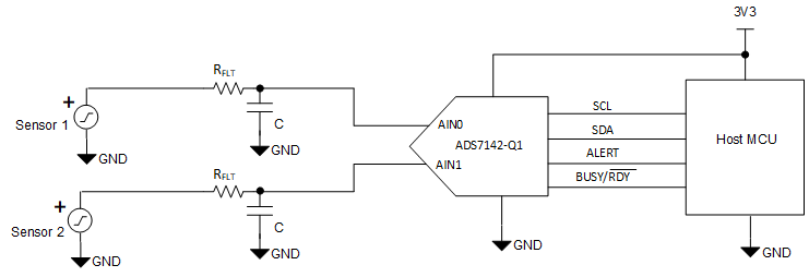
Automotive systems often require a device that monitors either critical voltage rails, temperature of the critical blocks or sensors, and gives an alert or interrupt to the host MCU only when the input being monitored crosses a predefined, programmable threshold. The ADS7142-Q1 is an excellent fit for such system level monitoring because this device can autonomously monitor sensor outputs and can wake up the host controller whenever the sensor output crosses predefined thresholds. Additionally, the ADS7142-Q1 has an internal data buffer that can store 16 sample data that can read in case further analysis is required. Figure 8-2 shows a typical block diagram of the ADS7142-Q1 as a sensor monitor. As is shown in this figure, the sensor can be connected directly to the input of the ADC (depending on the sensor output signal characteristics).
 Figure 8-2 Sensor
Monitor Circuit With the ADS7142-Q1