SBOA176E december 2016 – april 2023 INA240 , INA240-Q1 , INA253 , INA253-Q1 , INA254 , INA296A , INA296B , LMP8481 , LMP8481-Q1 , LMP8601 , LMP8601-Q1 , LMP8602 , LMP8602-Q1 , LMP8603 , LMP8603-Q1
There are many different switching power supply topologies available to meet system power requirements. DC–DC switching converters reduce a higher voltage DC rail to a lower voltage DC rail. These converter architectures include buck, boost, buck-boost, and flyback topologies. DC–AC switching converters convert a DC input voltage to an AC output voltage.
As implied by their name, switching converters employ various switches, transistors/FETs and/or diodes, to translate the input voltage to the desired output voltage at high system efficiency levels. The switching nature of these converters present challenges in trying to accurately measure the current waveforms. Voltage node requirements, system control requirements, and measurement drift are areas to consider when selecting current sense amplifiers.
Voltage Node Requirements
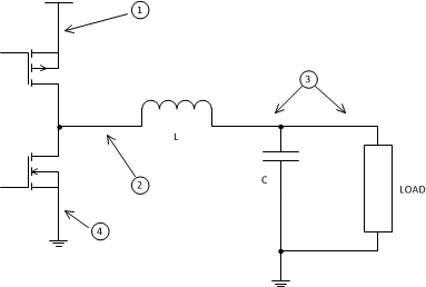
Each node in the circuit architecture has a different common-mode voltage and behavior. Measuring currents at each of these locations has different characteristics that the measurement circuit must take into consideration. Figure 1 illustrates the different nodes of a buck/step-down converter. The circuit shows a basic circuit consisting of a half H–bridge output stage with a low-pass filter constructed from an inductor and capacitor. The control circuitry, output stage drivers, and load are not shown.
 Figure 1 DC–DC Switching Power Supply – Buck
Architecture
Figure 1 DC–DC Switching Power Supply – Buck
ArchitectureNode 1 voltage is tied to the input supply of the converter. This is the high voltage the converter is “stepping-down” to the lower output voltage. Current measurements at this node are measuring the current flowing through the high-side devices of the half H–bridge and are used primarily for overcurrent/short–circuit detection with a comparator. Any measurements being made at this node require high common-mode circuits with the performance to measure a small differential voltage.
Node 2 is the mid-point of the half H–bridge and displays the pulse-width modulation (PWM) signal that switching power supplies are based upon. Current measurements here provide the inductor current for system control and overcurrent or short–circuit detection. The voltage transitions between the upper voltage and ground (or negative supply) in the PWM ratio are averaged to produce the correct output voltage. Node 2 voltage has sharp common-mode transitions, so measurements must be able to handle the transition voltage in magnitude as well as suppressing the transient in the output waveform.
Node 3 voltage is the converter output voltage, which is a DC voltage level with a small voltage ripple when observed on oscilloscope. Measurements at this location have similar requirements to Node 1 and provide the inductor current for use in system control and overcurrent or short-circuit detection. Even though Node 3 voltage is less than Node 1, the desired output voltage level can still require measurement circuitry to handle a high common-mode voltage.
Node 4 voltage is tied to ground of the circuit. This node detects low, close to ground, common-mode levels so measurements at this location have a reduced set of requirements compared with the previously-mentioned locations.
Other DC–DC switching architectures have similar behavior as Nodes 1 – 4, although they can be at different locations in the converter circuitry.
Measurement Drift Requirements
Switching power supplies are highly efficient circuits for voltage level translation, but there are still power losses in the conversion. These power losses are system efficiency losses that manifest as thermal generation or heat. Depending on the power levels of the converter, this can be a significant thermal source.
The INA240 has a-low thermal drift spec, which means that the current measurement does not change significantly due to heat generation. To further reduce the heat generated, the INA240 comes in different gain versions, which allow for the decrease in value of the current sense resistor. Traditional amplifiers can have significant decreases in performance as amplifier gain increases. By contrast, all gains versions of the INA240 have excellent electrical specifications allowing the achievement of high performance levels across different gain variants. Table 1 provides a comparison of the power dissipation difference between gains.
| Parameter | Gain | ||
|---|---|---|---|
| 20 V/V | 100 V/V | 200 V/V | |
| Input Voltage (mV) | 150 | 30 | 15 |
| RSENSE (mΩ) | 15 | 3 | 1.5 |
| Power dissipated (W) | 1.5 | 0.30 | 0.15 |
System Control and Monitoring Requirements
Most switching power supplies employ closed-feedback systems to provide stable, well regulated power. To provide optimized feedback control, precision measurements are desired. Amplifier specifications, like offset and gain errors, can significantly influence the regulation ability of the control system. Different feedback methods are used depending on the system requirements and desired complexity of the circuitry. Additionally, system power monitoring is a growing need as designs optimize and report the power consumption during different operating modes of the end equipment.
Voltage mode feedback compares a scaled version of the output voltage to a reference voltage to obtain the error voltage. This feedback method is relatively simple, but provides slow feedback as the system must allow the output voltage to change before adjustments can be made. Current measurements for voltage mode feedback generally monitor the load currents and determine if any short-circuits are present. The most important current amplifier criteria for voltage mode feedback converters is the common-mode output voltage of the converter. The output voltage on these converters ranges from low voltages used for microprocessors and low voltage digital circuitry (1.8 V to 5 V) to high voltages used for 48 V or higher systems. The output waveform, while after the filter, can still contain noise or transients that can disturb or cause errors in the measurement.
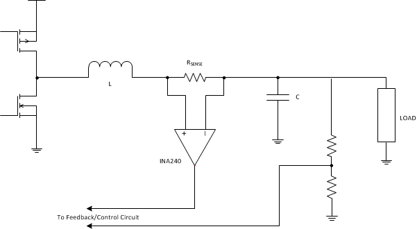
Current mode feedback adds a feedback loop to the control system that utilizes the system current. The current typically used is the inductor current in the converter (see Figure 2). This provides a much faster internal loop to run in parallel with the voltage feedback loop. In general, one of the down sides of current mode feedback is the susceptibility to noise/transients on the signal.
 Figure 2 Current Sensing for Power Supply Control
Feedback
Figure 2 Current Sensing for Power Supply Control
FeedbackCurrent mode feedback is generally split into peak current mode control and average current mode control. Peak current mode control utilizes the inductor current directly and therefore any noise or transients on the signal cause disturbances in the feedback loop. The INA240 is designed with high CMRR, which helps to attenuate any potential disturbances or noise due to the input signal.
Alternative Device Recommendations
Based on the system requirements, additional devices are available that can provide the needed performance and functionality. For applications requiring lower performance levels than the INA240, use the INA296B which has a higher common-mode input range or the INA290 for applications that do not require bidirectional current measurement. The INA253 and INA254 have integrated shunt resistors to provide a tuned system approach.
| Device | Optimized Parameters | Performance Trade-Off |
|---|---|---|
| INA253 | Integrated Low-Inductive Shunt: 2 mΩ, PWM rejection | ±15 A at TA = 85°C |
| INA254 | Integrated Low-Inductive Shunt: 400-µΩ, PWM rejection | ±50 A at TA = 85°C |
| INA296B | Bidirectional, Wider Common-Mode Input range, Small SOT-23 | No Enhanced PWM Rejection |
| INA290 |
Unidirectional up to 120 V |
No Enhanced PWM Rejection |