SBOA187E december 2020 – april 2023 INA240 , INA240-Q1 , INA241A , INA241B , INA253 , INA253-Q1 , INA254 , INA282 , INA282-Q1 , INA283 , INA283-Q1 , INA284 , INA284-Q1 , INA285 , INA285-Q1 , INA286 , INA286-Q1 , INA296A , INA296B , LMP8481 , LMP8481-Q1
Application Brief
Most switching power supplies are designed with closed-loop feedback circuitry to provide stable power under various transient and load conditions. The feedback methodology options fall into two general categories, voltage mode control (VMC), and current mode control (CMC). Both methodologies have their strengths and weakness that determine the appropriate selection for the end-equipment application.
Control Methodologies
Voltage mode control utilizes a scaled value of the output voltage as the feedback signal. This methodology provides simple, straight-forward feedback architecture for the control path. There are several disadvantages that arise from using this method. The most significant disadvantage is output voltage regulation requires sensing a change in output voltage and propagation through the entire feedback signal and filter before the output is appropriately compensated. This can generate a unacceptably slow response for systems that need high levels of regulation. The feedback compensation of the supply requires a higher level of analysis to address the two poles introduced by the output low-pass filter. Additionally, the feedback component values must be adjusted since different input voltages affect the overall loop gain.
Current mode control addresses the previously-mentioned shortfalls of voltage mode control by using the inductor current waveform for control. This signal is included with the output voltage feedback loop as a second, fast response control loop. The additional feedback loop does potentially increase the circuit/feedback complexity, so the advantages need to be evaluated as part of the design requirements.
By using the inductor current as part of the feedback control:
- The added current feedback loop responds faster compared with only using the output voltage for feedback control. Additionally, with the inductor current information, the circuit can be designed to provide pulse by pulse current limiting allowing rapid detection and control for current-limiting needs.
- The power supply looks like a voltage controlled current source. This permits a modular supply design to allow load sharing between multiple supplies in a parallel configuration.
- The effects of the inductor in the control loop can be minimized since the current feedback loop effectively reduces the compensation to a single pole requirement.
While current mode control addresses some of the drawbacks of VMC, it introduces challenges that can effect the circuit performance. The addition of the current feedback loop increases the complexity of the control/feedback circuit and circuit analysis. Stability across the entire range of duty cycles and sensitivity to noise signals are other items that need to be considered in the selection of current mode control. CMC can further be broken down into several different types of control schemes: peak, valley, emulated, hysteretic, and average CMC. The following text covers the two most common methodologies used in circuit design — peak and average current mode control.
Peak Current Mode Control
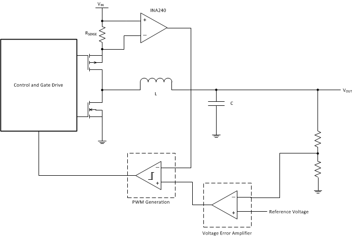
Peak current mode control (PCMC) utilizes the current waveform directly as the ramp waveform into the PWM-generation comparator instead of a externally generated sawtooth- or triangle-signal like VMC. The up-slope portion of the inductor current or high-side transistor current waveform is used to provide a fast response control loop in addition to the existing voltage control loop. As shown in Figure 1, the current signal is compared with the output of the voltage error amplifier to generate the PWM control signal for the power supply.
 Figure 1 PCMC Circuit Block Diagram
Switching power supplies provide high levels of efficiency between the input and output power rails. To maintain the high efficiency of the converter, ideally the sense resistor used to measure the inductor current is as small as possible to reduce power loss due to the measurement. This small-valued resistor results in a small amplitude feedback signal. Since the inductor current waveform is used directly as the comparator input signal, PCMC is known to be susceptible to noise and voltage transients. Using a current-sense amplifier like the INA240 with high common-mode rejection ratio (CMRR) provides suppression of transients associated with pulse-width modulation (PWM) signals and systems. The gain flexibility of the INA240 allows the inductor current waveform be amplified to provide a larger signal for comparison without the need for additional gain or sacrificing performance. Additionally, the low offset and gain errors provide a reduction in design variations and changes across temperature. To utilize PCMC, the inductor current necessitates a high common-mode voltage measurement. The INA240 common-mode range allows for a wide range in supply input and output voltages.
Note that PCMC most often adds slope compensation to address stability issues with duty cycles greater than 50%. The slope compensation is added to the inductor current before being used as the comparator input signal.
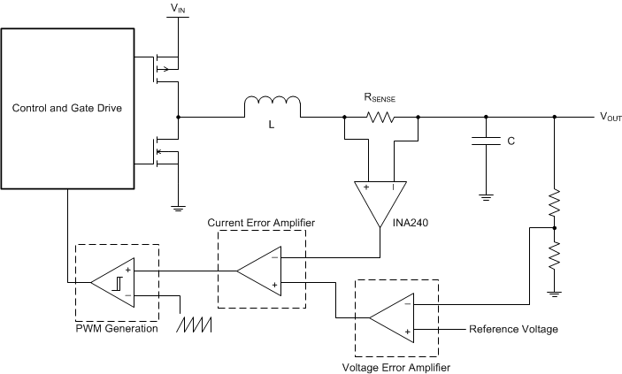
 Figure 2 ACMC Circuit Block Diagram
Average Current Mode Control
Average current mode control (ACMC) utilizes the inductor current waveform and an additional gain and integration stage before the signal is compared to a externally provided ramp waveform (similar to VMC). This allows improved immunity to noise and removes the need for slope compensation. Figure 2 shows a block diagram of ACMC operation for a buck converter.
The noise sensitivity of PCMC methodology is improved using ACMC to acceptable performance levels with the INA240 high CMRR helping to provide additional transient reduction. The INA240 high common-mode range is required to make the inductor current measurement and allows usage of the current amplifier in a wide-range of output voltages. The INA240 high accuracy and low drift specifications provide consistent measurement across temperature and different assemblies.
The INA240 provides performance and features for measurement accuracy which is needed to maintain good control signal integrity. The INA240 features a 25-μV maximum input offset voltage and a 0.20% maximum gain error specification at room temperature. Temperature stability is important to maintain system performance and the INA240 provides input offset voltage drift of 250 nV/°C with a 2.5 ppm/°C amplifier gain drift. The INA240 features enhanced PWM rejection to improve performance with large common-mode transients and a wide common-mode input range for maximum design variance for supply output voltages.
Alternative Device Recommendations
Based on system requirements, alternative devices are available that can provide the needed performance and functionality. For applications with voltages up to 110 V and fast settling requirements, using the INA296B with high bandwidth is a great choice for a dedicated current-sense amplifier. The INA241B also provides an input common-mode voltage range reaching up to 110 V and features enhanced PWM rejection circuitry for applications with large common-mode input voltage transitions, such as motor control and switching power supplies.
| Device | Optimized Parameters | Performance Trade-Off |
|---|---|---|
| INA296B | Bidirectional, Wider Common-Mode Input Range, Small Package (SOT-23) | No Enhanced PWM Rejection |
| INA241B | Bidirectional, Wider Common-Mode Input Range, Enhanced PWM Rejection, Small Package (SOT-23) | Increased IQ |