SBOA293A December 2018 – January 2021 TLV9002
Design Goals
| Input | Output | BW | Supply | |||
|---|---|---|---|---|---|---|
| ViMin | ViMax | VoMin | VoMax | fp | Vee | Vcc |
| –0.1V | 0.1V | –2V | 2V | 2kHz | –2.5V | 2.5V |
Design Description
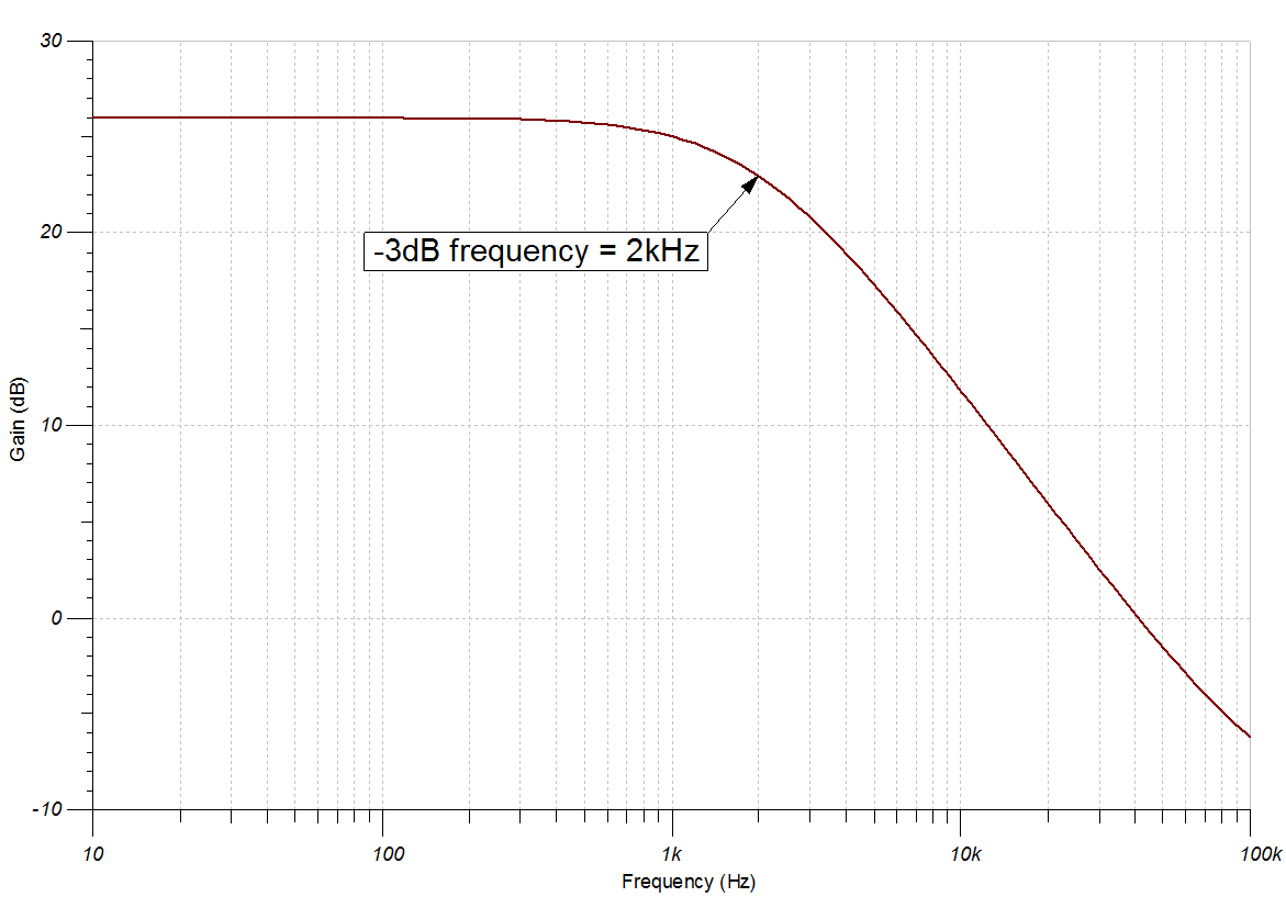
This tunable low–pass inverting amplifier circuit amplifies the signal level by 26dB or 20V/V. R2 and C1 set the cutoff frequency for this circuit. The frequency response of this circuit is the same as that of a passive RC filter, except that the output is amplified by the pass–band gain of the amplifier. Low–pass filters are often used in audio signal chains and are sometimes called bass–boost filters.
Design Notes
- C1 and R2 set the low–pass filter cutoff frequency.
- The common-mode voltage is set by the non–inverting input of the op amp, which in this case is mid–supply.
- Using high value resistors can degrade the phase margin of the circuit and introduce additional noise in the circuit.
- R2 and R1 set the gain of the circuit.
- The pole frequency fp of 2kHz is selected for an audio bass–boost application.
- Avoid placing capacitive loads directly on the output of the amplifier to minimize stability issues.
- Large signal performance may be limited by slew rate. Therefore, check the maximum output swing versus frequency plot in the data sheet to minimize slew–induced distortion.
- For more information on op amp linear operation region, stability, slew–induced distortion, capacitive load drive, driving ADCs and bandwidth please see the design references section.
Design Steps
The DC transfer function of this circuit is given below.

- Pick resistor values for given passband gain. Equation 1.
 Equation 1.
 Equation 1.
- Select low–pass filter pole frequency fpEquation 1.

- Calculate C1 using R2 to set
the location of fp. Equation 1.
 Equation 1.
- Calculate the minimum slew rate required to minimize slew–induced distortion. Equation 1.
 Equation 1.
- SRTLV9002 = 2V/µs, therefore it meets this requirement
Design Simulations
AC Simulation Results
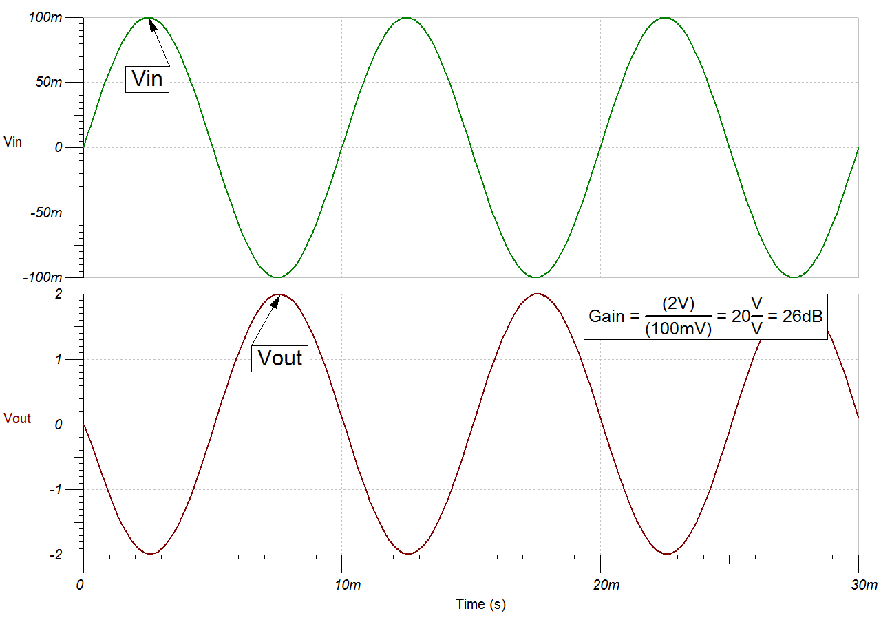
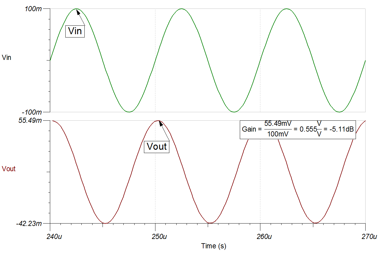
Transient Simulation Results
A 100 Hz, 0.2 Vpp sine wave yields a 4 Vpp output sine wave.
A 100 kHz, 0.2 Vpp sine wave yields a 0.1 Vpp output sine wave.
References:
- Analog Engineer's Circuit Cookbooks
- SPICE Simulation File SBOC523
- TI Precision Designs TIPD185
- TI Precision Labs
Design Featured Op Amp
| TLV9002 | |
|---|---|
| Vss | 1.8V to 5.5V |
| VinCM | Rail–to–rail |
| Vout | Rail–to–rail |
| Vos | 0.4mV |
| Iq | 60µA |
| Ib | 5pA |
| UGBW | 1MHz |
| SR | 2V/µs |
| #Channels | 1,2,4 |
| www.ti.com/product/tlv9002 | |
Design Alternate Op Amp
| OPA375 | |
|---|---|
| Vss | 2.25V to 5.5V |
| VinCM | Vee to Vcc –1.2V |
| Vout | Rail–to–rail |
| Vos | 0.15mV |
| Iq | 890µA |
| Ib | 10pA |
| UGBW | 10MHz |
| SR | 4.75V/µs |
| #Channels | 1 |
| www.ti.com/product/opa375 | |
| Revision | Date | Change |
|---|---|---|
| A | January 2021 | Updated result in Design Step 4 from 0.25 to 0.025 |