SBOA300A June 2018 – December 2020 INA181 , INA181-Q1 , INA186 , INA186-Q1 , INA190 , INA190-Q1 , INA199 , INA199-Q1 , INA210 , INA210-Q1 , INA211 , INA211-Q1 , INA212 , INA212-Q1 , INA213 , INA213-Q1 , INA214 , INA214-Q1 , INA215 , INA215-Q1 , INA2181 , INA2181-Q1 , INA4181 , INA4181-Q1
Design Goals
| Input | Output | Supply | ||||
|---|---|---|---|---|---|---|
| IinMin | IinMax | Vcm | VoutMin | VoutMax | Vs | Vref |
| –4A | 4A | 12.5 V | 0.5 V | 4.5 V | 5 | 2.5 V |
Design Description
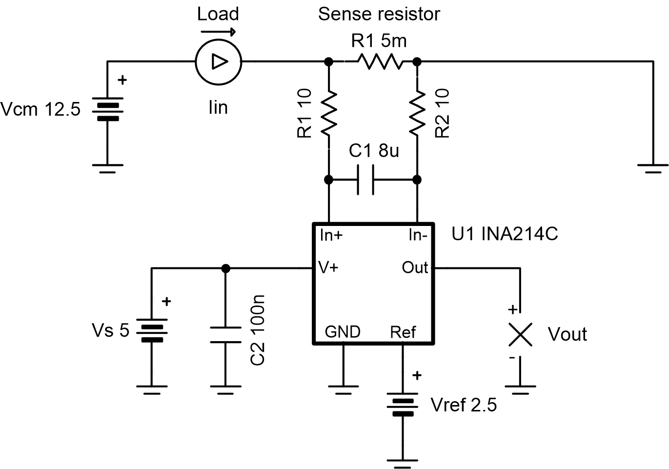
The low-side bidirectional current-shunt monitor solution illustrated in the following image can accurately measure currents from –4A to 4A, and the design parameters can easily be changed for different current measurement ranges. Current-shunt monitors from the INA21x family have integrated precision gain resistors and a zero-drift architecture that enables current sensing with maximum drops across the shunt as low as 10mV full-scale.
Design Notes
- To avoid additional error, use R1 = R2 and keep the resistance as small as possible (no more than 10Ω, as stated in INA21x Voltage Output, Low- or High-Side Measurement, Bidirectional, Zero-Drift Series, Current-Shunt Monitors).
- Low-side sensing should not be used in applications where the system load cannot withstand small ground disturbances or in applications that need to detect load shorts.
- The Getting Started with Current Sense Amplifiers video series introduces implementation, error sources, and advanced topics that are good to know when using current sense amplifiers.
Design Steps
- Determine Vref based on
the desired current range:
With a current range of –4A to 4A, then half of the range is below 0V, so set:
Equation 1. - Determine the desired shunt
resistance based on the maximum current and maximum output voltage:
To not exceed the swing-to-rail and to allow for some margin, use VoutMax = 4.5V. This, combined with maximum current of 4A and the Vref calculated in step 1, can be used to determine the shunt resistance using the equation:
Equation 1. - Confirm Vout will be
within the desired range:
At the maximum current of 4A, with Gain = 100V/V, R1 = 5mΩ, and Vref = 2.5V:
Equation 1.At the minimum current of -4A, with Gain = 100V/V, R1 = 5mΩ, and Vref = 2.5V:
Equation 1. - Filter cap selection:
To filter the input signal at 1kHz, using R1 = R2 = 10Ω:
Equation 1.
For more information on signal filtering and the associated gain error, see INA21x Voltage Output, Low- or High-Side Measurement, Bidirectional, Zero-Drift Series, Current-Shunt Monitors.
Design Simulations
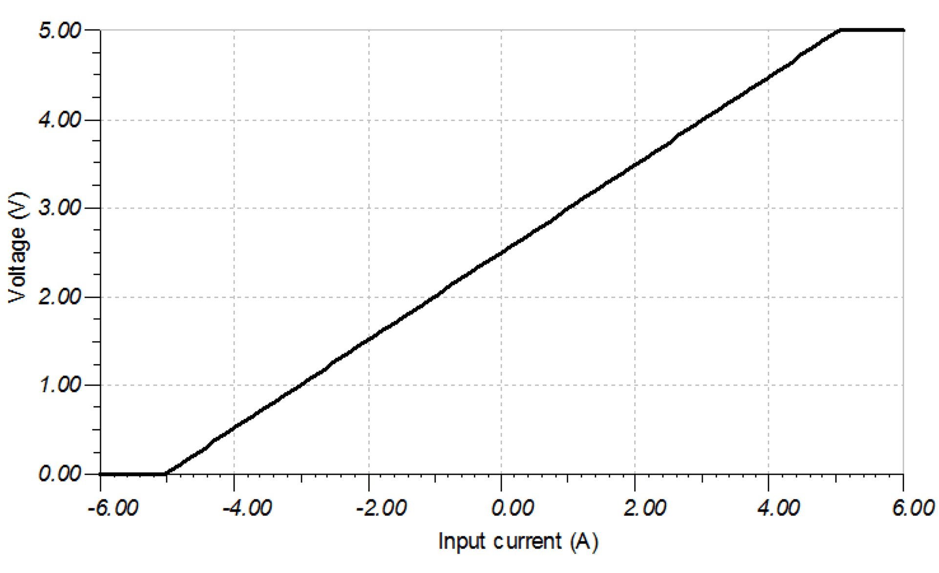
DC Analysis Simulation Results
The following plot shows the simulated output voltage Vout for the given input current Iin.
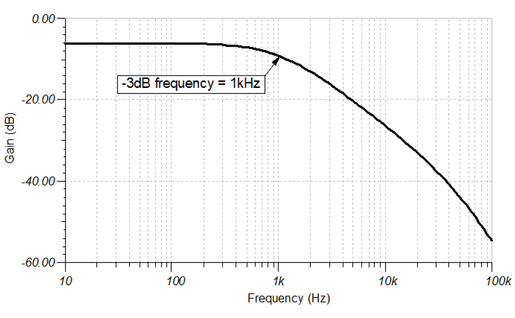
AC Analysis Simulation Results
The following plot shows the simulated gain vs frequency, as designed for in the design steps.
Transient Analysis Simulation Results
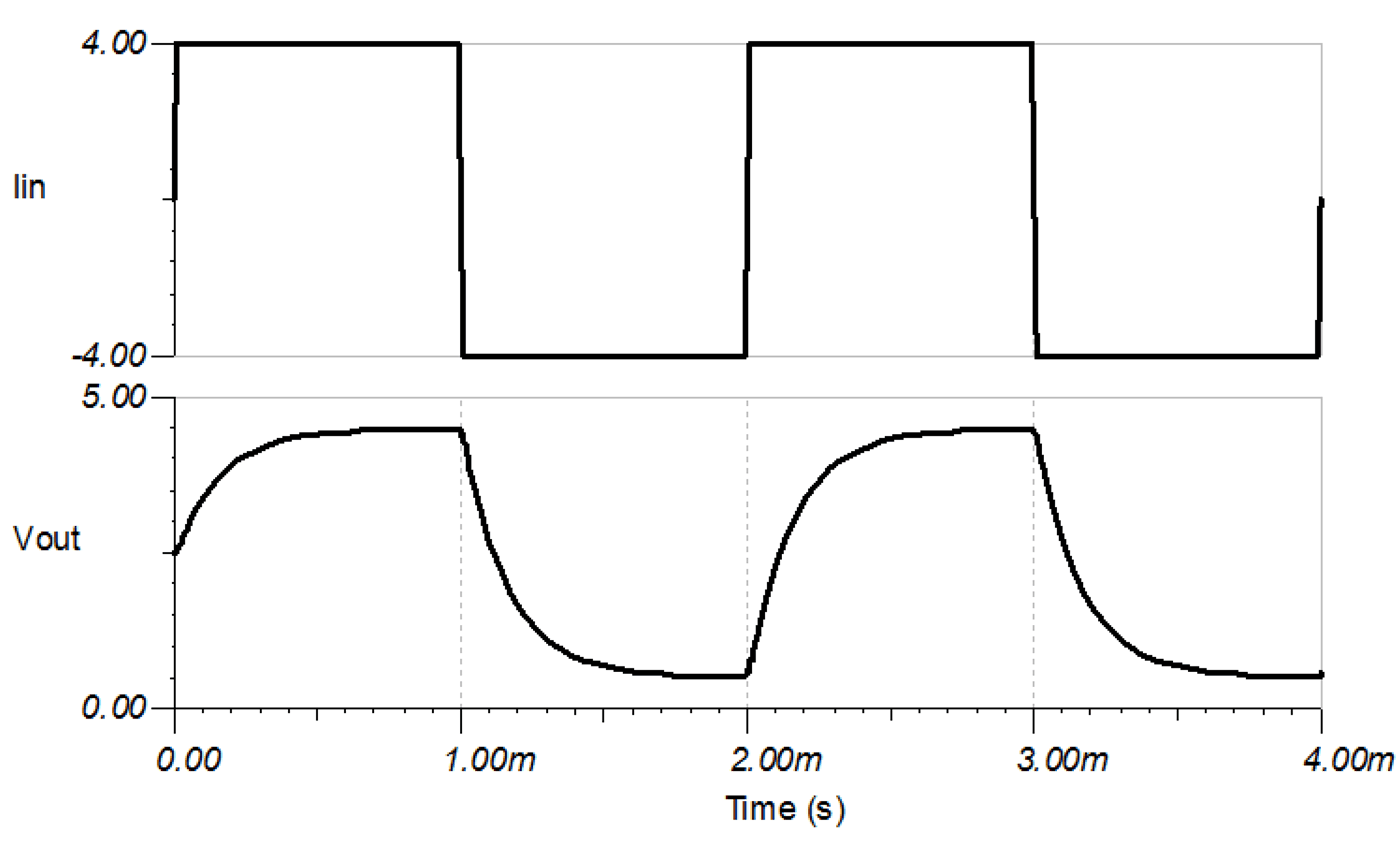
The following plot shows the simulated delay and settling time of the output Vout for a step response in Iin from –4A to 4A.