SBOA400 July 2020 – MONTH TMCS1100 , TMCS1100-Q1 , TMCS1101 , TMCS1101-Q1 , TMCS1107 , TMCS1107-Q1 , TMCS1108 , TMCS1108-Q1
3 ESD Body Diode Characterization
Measuring die temperature is achieved by forward biasing one of the device’s internal ESD diodes while the low voltage side is not powered. The voltage seen across the diode changes according to cumulative temperature from heat sources internal and external to the device. By forcing the device to a known temperature without passing a load through the device, the diode voltage to temperature relationship can be determined.
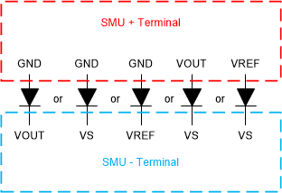
Each diode shown in Figure 3-1 can individually be forward biased by forcing current from a source measure unit (SMU) (+) terminal into the anode, through to the respective cathode, and out to the SMU (–) terminal. For this application report, the diode forward biased from GND to VOUT was used, while VS and VREF were left floating. To force current, a Keithley 2420 source meter was used. To use the diode for temperature measurements, the forced current should be sufficient for the voltage across the ESD diode to reach the forward voltage, but not exceed the device max quiescent current of 6 mA. Consequently 1 mA was used for the tests in this report as the current level satisfies both conditions. To characterize the device across temperature an oven or bath can be used. For the diodes characterized in this report, multiple TMCS1100 devices were placed in a Harte Scientific oil bath and swept across temperature with measurements at 25°C, 75°C, 100°C, and 125°C.
 Figure 3-1 TMCS1100 ESD Diodes
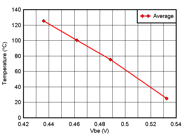
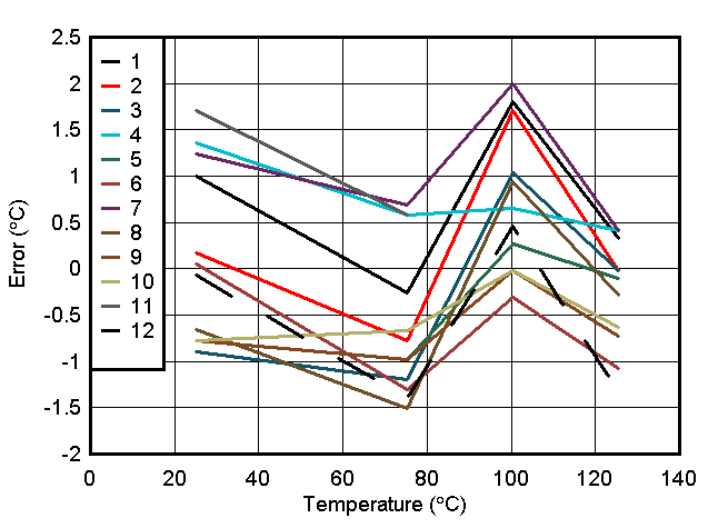
From the temperature sweeps, 12 data curves were collected. From those curves an average curve shown in Figure 3-2 was derived with corresponding best fit Equation 2. Comparing the average to the actual measured data indicates that there will be some error in calculation when using the equation as shown in Figure 3-3. While the equation provides ±2°C tolerance for the characterized device diodes in this application report, different forcing currents and different device lots may be better characterized by another equation. Therefore, if precision is desired, we recommend characterizing the diodes for your devices.
 Figure 3-2 Diode Voltage Versus
Temperature
 Figure 3-3 Temperature Error
Step Summary
- Apply SMU positive terminal to device ground pin and SMU negative terminal to device Vout pin.
- Immerse devices in a temperature controllable chamber.
- Source 1mA of current to GND pin from source meter.
- Measure voltage across body diode, in this case GND to VOUT.
- Sweep DUT through series of temperatures.
- Take average of each temperature step and plot.
- Determine best fit equation for plotted line.