SBOA510 March 2021 OPA455 , OPA462
- Trademarks
- 1Introduction
- 2Three Op Amp OPA462 HV Solution
- 3Lower Voltage, Lower Cost Three Op Amp Solution
- 4OPA462 300 Vpp Output Solution With Discrete Transistor Supply-Rail Drivers
- 5Lessons Learned from the Practical Implementation of the HV Op Amp Solutions
-
A Appendix
- A.1 Overview
- A.2 Summary of Results
- A.3 Test Setup and Equipment
- A.4 Printed Circuit Boards
- A.5 Power Supply, Source Measurement Unit (SMU)
- A.6 Arbitrary Waveform Generator (AWG)
- A.7 Oscilloscope
- A.8 Circuit 1: OPA462 Three op amp Solution
- A.9 Circuit 2: Lower Voltage, Lower Cost Three Op Amp Solution
- A.10 Circuit 3: OPA462 300 Vpp Output Solution With Discrete Transistor Supply-Rail Drivers
A.3 Test Setup and Equipment
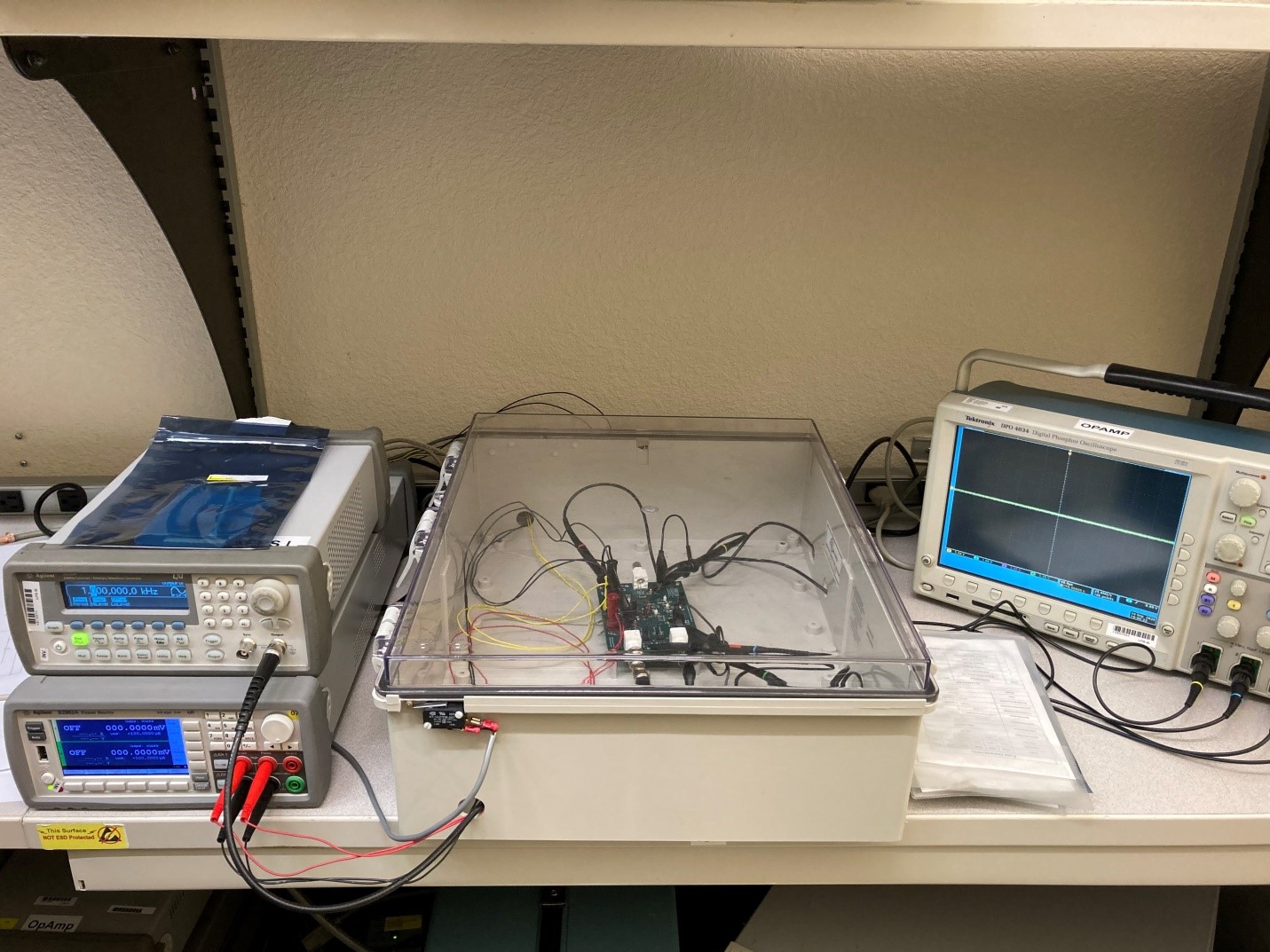
Figure 6-1 shows the benchtop test setup.
WARNING: Exercise extreme caution when working with high voltages! Injury or
death could result from improper handling or usage of high-voltage circuits.
The HV circuits are enclosed in an HV interlock box that has safety switches which trip to turn off the HV power when the lid to the box is opened.
 Figure 6-1 Benchtop Test Setup