SBOA510 March 2021 OPA455 , OPA462
- Trademarks
- 1Introduction
- 2Three Op Amp OPA462 HV Solution
- 3Lower Voltage, Lower Cost Three Op Amp Solution
- 4OPA462 300 Vpp Output Solution With Discrete Transistor Supply-Rail Drivers
- 5Lessons Learned from the Practical Implementation of the HV Op Amp Solutions
-
A Appendix
- A.1 Overview
- A.2 Summary of Results
- A.3 Test Setup and Equipment
- A.4 Printed Circuit Boards
- A.5 Power Supply, Source Measurement Unit (SMU)
- A.6 Arbitrary Waveform Generator (AWG)
- A.7 Oscilloscope
- A.8 Circuit 1: OPA462 Three op amp Solution
- A.9 Circuit 2: Lower Voltage, Lower Cost Three Op Amp Solution
- A.10 Circuit 3: OPA462 300 Vpp Output Solution With Discrete Transistor Supply-Rail Drivers
4 OPA462 300 Vpp Output Solution With Discrete Transistor Supply-Rail Drivers
Certainly, cost and complexity are always considerations in any design. The next solution aims at reducing both while maintaining the high performance of the OPA462 as the signal amplifier. If the OPA462 U2, U3 rail drivers can be replaced with low-cost discrete HV bipolar transistors, or HV MOSFETS, a simpler, lower cost 300-Vpp output solution may be realized.
Life teaches us "there is no such thing as a free lunch" and in this case for a lower cost solution that old phrase lends merit. This circuit applies discrete transistors in place of the op amps at U2 and U3. Like the op amps, the transistors function as voltage followers, but lack the local feedback and rejection characteristics (PSRR, CMRR) op amps exhibit and employ to enhance precision circuit performance. These op amp electrical characteristics are responsible for reducing errors to very low levels and that is not the case for the simple discrete replacements. Although the discrete followers work well in this third circuit implementation the price to be paid is in less precise DC performances.
High-voltage MOSFETs, bipolar transistors, and Darlington bipolar transistors were all considered as supply-rail driver replacements for the U2 and U3 op amp circuit positions. When the electrical aspects of the supply-rail drivers were fully considered and tested, the HV Darlington transistors were found to provide both ease of use and highly predictable electrical performance. This is not implying conventional HV bipolar transistors and MOSFETS are not usable, it simply was observed that the Darlington’s performance on the bench more closely followed the theoretical and simulated performances than was the case for the other types of transistors.
Darlington transistors have an advantage of much higher current gain (β) than conventional transistors. Simplistically, it is like two cascaded transistors connected base-emitter driving another base-emitter where the total βT equals β1 × β2. If β1 = β2, then β2 results. That significantly decreases the base current (Ib) that flows through the output resistor dividers and results in a more predictable voltage at the resistor divider points Vi2 and Vi3. The HV MOSFETs, while presenting extremely high impedance to the dividers, can have a widely varying gate-to-source threshold voltage (VTH) from one device to the next. Additionally, the availability of HV, low-current MOSFETs is quite limited and their drain-to-source ON resistance RDS(ON) tends to be high compared to their high-current counterparts. High RDS(ON) can result in a larger voltage drop across the drain to source of the MOSFET that reduces the voltage at the U1 supply pins when maximum output current is required by the load.
A good choice for the high-voltage Darlington transistors well suited for this HV op amp application are manufactured by Diodes Incorporated, the ZXTN04120HFF NPN and ZXTP05120HFF PNP. Both have a BVCEO > 120 V. The op amp circuit power supply should be kept to a maximum of about ±155 V when the full swing of the OPA462 output range and the 120 V BVCEO are both taken into full consideration.
The basic design using a Darlington bipolar transistor for the OPA462 supply pin driver is seen in the Figure 4-1 partial circuit schematic. The NPN Darlington transistor T1 is connected as an emitter follower providing the supply voltage to the Vp pin of the U1. A complementary PNP Darlington is employed at its Vn pin.
 Figure 4-1 Darlington Transistor Driver for
U1 OPA462 Positive Supply pin
Figure 4-1 Darlington Transistor Driver for
U1 OPA462 Positive Supply pinThe voltage appearing at the OPA462 positive supply pin Vp is determined from the loop equation:
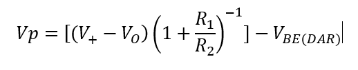
Where VBE(DAR) is the sum of the VBE voltage of the two integrated transistors that make up the Darlington transistor.
If the desired value for Vp is decided upon, then Equation 1 can be rearranged to provide resistor values for R1 or R2. To find R1, select a value for R2 that sets the Vo to midscale, or in this example 0 V. A 100-kΩ resistor value is a practical value for R2 in this application circuit. Then calculate R1 from:
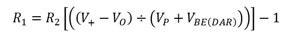
For example, if the desired V+ is 90 V, Vp is 155 V, R2 is selected to be 100 kΩ, and with VBE(DAR) approximated to be 1.4 V, then R1 derived from Equation 2 is:
R1 = 1 × 10⁵ Ω [((155 V – 0 V) / (90 V + 1.4 V)) – 1 V] = 69.6 × 10⁴ Ω ≈ 70 kΩ
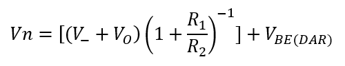
The Darlington PNP complement to the NPN in Figure 4-2 circuit is used to create Vn. Vn is created in the same way as Vp, but instead utilizing the negative polarities:
The two simple Darlington voltage followers develop and provide a reasonably constant 180 V across the OPA462 U1 supply pins. Bench measurements indicate that the voltage control is not quite as tight as with the U2, U3 op amp circuits, but it is completely satisfactory for many applications.
Figure 4-2 shows a practical application of a high-voltage amplifier circuit where the Darlington transistors provide the supply voltages and current to U1, the OPA462 signal amplifier.
Observe that the OPA462 supply pins do not have the commonly included power supply bypass capacitors from the Vp and Vn pins to ground. Instead, bypassing is primarily accomplished by a 10-nF capacitor is connected between the NPN and PNP Darlington transistor bases whose emitters drive the supply pins of U1.
The base-to-base capacitance of the capacitor becomes multiplied by the Darlington’s βT. The result is an equivalent capacitance across the supply pins of the U1 that is βT × C, or several thousand times the 10-nF value of the capacitor. The equivalent capacitor exhibits a very low impedance across the U1 supply pins down to low frequencies. Additionally, the impedance looking into the Darlington transistor emitter followers is very low and that parallels the very low reactance of the equivalent capacitor. The net result is a very low impedance supply bypass effective to very low frequencies.
 Figure 4-2 Darlington Transistor Supply-Rail Drivers for OPA462, 310-V Total Supply
A TINA Spice circuit simulation with ±155-V supplies yields base voltages of 91.2 V for the NPN, and –91.2 V for the PNP when the output voltage of the U1 is at 0 V. The Darlington transistor emitters are two base-emitter drops below and above their bases at 90.1 V for the NPN, and –90 V for the PNP. This configuration results in 180 V across the supply pins of U1. Like the previous two circuits, the supply pins of U1 track with the U1 output voltage level.