SBOS629B April   2018  – May 2025 OPA858

PRODUCTION DATA  

  1.   1
  2. Features
  3. Applications
  4. Description
  5. Device Comparison Table
  6. Pin Configuration and Functions
  7. Specifications
    1. 6.1 Absolute Maximum Ratings
    2. 6.2 ESD Ratings
    3. 6.3 Recommended Operating Conditions
    4. 6.4 Thermal Information
    5. 6.5 Electrical Characteristics
    6. 6.6 Typical Characteristics
  8. Parameter Measurement Information
  9. Detailed Description
    1. 8.1 Overview
    2. 8.2 Functional Block Diagram
    3. 8.3 Feature Description
      1. 8.3.1 Input and ESD Protection
      2. 8.3.2 Feedback Pin
      3. 8.3.3 Wide Gain-Bandwidth Product
      4. 8.3.4 Slew Rate and Output Stage
      5. 8.3.5 Current Noise
    4. 8.4 Device Functional Modes
      1. 8.4.1 Split-Supply and Single-Supply Operation
      2. 8.4.2 Power-Down Mode
  10. Application and Implementation
    1. 9.1 Application Information
      1. 9.1.1 Using the OPA858 as a Transimpedance Amplifier
    2. 9.2 Typical Applications
      1. 9.2.1 TIA in an Optical Front-End System
        1. 9.2.1.1 Design Requirements
        2. 9.2.1.2 Detailed Design Procedure
        3. 9.2.1.3 Application Curves
    3. 9.3 Power Supply Recommendations
    4. 9.4 Layout
      1. 9.4.1 Layout Guidelines
      2. 9.4.2 Layout Example
  11. 10Device and Documentation Support
    1. 10.1 Device Support
      1. 10.1.1 Development Support
    2. 10.2 Documentation Support
      1. 10.2.1 Related Documentation
    3. 10.3 Receiving Notification of Documentation Updates
    4. 10.4 Support Resources
    5. 10.5 Trademarks
    6. 10.6 Electrostatic Discharge Caution
    7. 10.7 Glossary
  12. 11Revision History
  13. 12Mechanical, Packaging, and Orderable Information

Typical Characteristics

at VS+ = 2.5 V, VS– = –2.5 V, VIN+ = 0 V, RF = 453 Ω, gain = 7 V/V, RL = 200 Ω, output load referenced to midsupply, and TA = 25°C (unless otherwise noted)

OPA858 Small-Signal Frequency
                        Response vs Gain
VOUT = 100 mVPP; see Figure 7-1 and Figure 7-2 for circuit configuration
Figure 6-1 Small-Signal Frequency Response vs Gain
OPA858 Small-Signal Frequency
                        Response vs Output Load
VOUT = 100 mVPP
Figure 6-3 Small-Signal Frequency Response vs Output Load
OPA858 Small-Signal Frequency
                        Response vs Capacitive Load
VOUT = 100 mVPP; see Figure 7-3 for circuit configuration
Figure 6-5 Small-Signal Frequency Response vs Capacitive Load
OPA858 Large-Signal Response for 0.1-dB Gain Flatness
VOUT = 2 VPP
Figure 6-7 Large-Signal Response for 0.1-dB Gain Flatness
OPA858 Closed-Loop Output Impedance vs Frequency
Small-signal response
Figure 6-9 Closed-Loop Output Impedance vs Frequency
OPA858 Voltage Noise Density vs Frequency
 
Figure 6-11 Voltage Noise Density vs Frequency
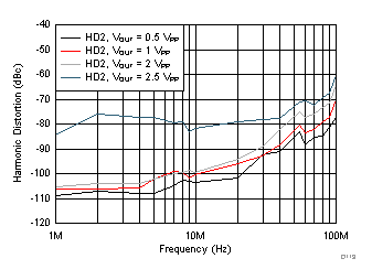
OPA858 Harmonic Distortion (HD2) vs Output Swing
 
Figure 6-13 Harmonic Distortion (HD2) vs Output Swing
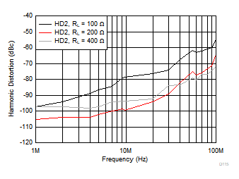
OPA858 Harmonic Distortion (HD2) vs Output Load
VOUT = 2 VPP
Figure 6-15 Harmonic Distortion (HD2) vs Output Load
OPA858 Harmonic Distortion (HD2) vs Gain
VOUT = 2 VPP
Figure 6-17 Harmonic Distortion (HD2) vs Gain
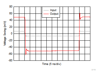
OPA858 Small-Signal Transient Response
Average rise-and-fall time (10%–90%) = 450 ps
Figure 6-19 Small-Signal Transient Response
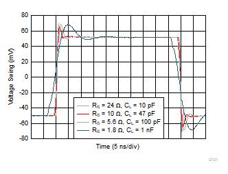
OPA858 Small-Signal Transient Response vs Capacitive Load
 
Figure 6-21 Small-Signal Transient Response vs Capacitive Load
OPA858 Turn-On Transient Response
VS+ = 5 V, VS– = ground
Figure 6-23 Turn-On Transient Response
OPA858 Common-Mode Rejection Ratio vs Frequency
Small-signal response
Figure 6-25 Common-Mode Rejection Ratio vs Frequency
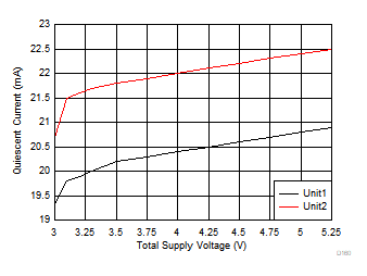
OPA858 Quiescent Current vs Supply Voltage
2 typical units
Figure 6-27 Quiescent Current vs Supply Voltage
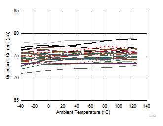
OPA858 Quiescent Current (Amplifier Disabled) vs Ambient Temperature
30 units tested
Figure 6-29 Quiescent Current (Amplifier Disabled) vs Ambient Temperature
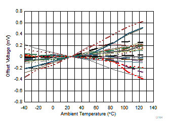
OPA858 Offset Voltage vs Ambient Temperature
µ = 1 µV/°C σ = 2.2 µV/°C 28 units tested
Figure 6-31 Offset Voltage vs Ambient Temperature
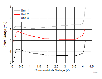
OPA858 Offset Voltage vs Input Common-Mode Voltage
VS = 5 V 3 typical units
Figure 6-33 Offset Voltage vs Input Common-Mode Voltage
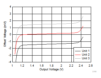
OPA858 Offset Voltage vs Output Swing
VS = 3.3 V 3 typical units
Figure 6-35 Offset Voltage vs Output Swing
OPA858 Offset Voltage vs Output Swing vs Ambient Temperature
 
Figure 6-37 Offset Voltage vs Output Swing vs Ambient Temperature
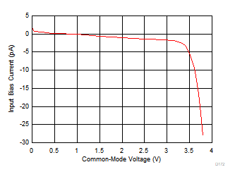
OPA858 Input
                        Bias Current vs Input Common-Mode Voltage
 
Figure 6-39 Input Bias Current vs Input Common-Mode Voltage
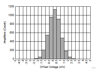
OPA858 Offset Voltage Distribution
µ = –0.28 mV σ = 0.8 mV 4555 units tested
Figure 6-41 Offset Voltage Distribution
OPA858 Small-Signal Frequency
                        Response vs Supply Voltage
VOUT = 100 mVPP
 
Figure 6-2 Small-Signal Frequency Response vs Supply Voltage
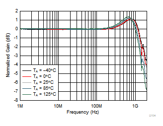
OPA858 Small-Signal Frequency
                        Response vs Ambient Temperature
VOUT = 100 mVPP
Figure 6-4 Small-Signal Frequency Response vs Ambient Temperature
OPA858 Large-Signal Frequency
                        Response vs Gain
VOUT = 2 VPP
Figure 6-6 Large-Signal Frequency Response vs Gain
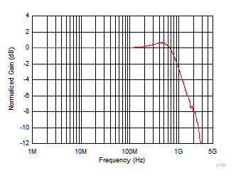
OPA858 Large-Signal Frequency Response
VS = 3.3 V VOUT = 1 VPP
Figure 6-8 Large-Signal Frequency Response
OPA858 Open-Loop Magnitude and Phase vs Frequency
Small-signal response
Figure 6-10 Open-Loop Magnitude and Phase vs Frequency
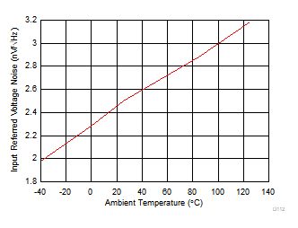
OPA858 Voltage Noise Density vs Ambient Temperature
Frequency = 10 MHz
Figure 6-12 Voltage Noise Density vs Ambient Temperature
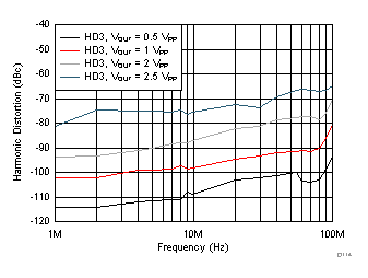
OPA858 Harmonic Distortion (HD3) vs Output Swing
 
Figure 6-14 Harmonic Distortion (HD3) vs Output Swing
OPA858 Harmonic Distortion (HD3) vs Output Load
VOUT = 2 VPP
Figure 6-16 Harmonic Distortion (HD3) vs Output Load
OPA858 Harmonic Distortion (HD3) vs Gain
VOUT = 2 VPP
Figure 6-18 Harmonic Distortion (HD3) vs Gain
OPA858 Large-Signal Transient Response
Average rise-and-fall time (10%–90%) = 750 ps
Figure 6-20 Large-Signal Transient Response
OPA858 Output Overload Response
2 × output overdrive
Figure 6-22 Output Overload Response
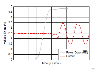
OPA858 Turn-Off Transient Response
VS+ = 5 V, VS– = ground
Figure 6-24 Turn-Off Transient Response
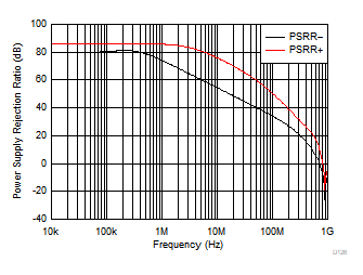
OPA858 Power
                        Supply Rejection Ratio vs Frequency
Small-signal response
Figure 6-26 Power Supply Rejection Ratio vs Frequency
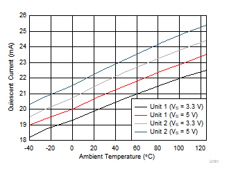
OPA858 Quiescent Current vs Ambient Temperature
2 typical units
Figure 6-28 Quiescent Current vs Ambient Temperature
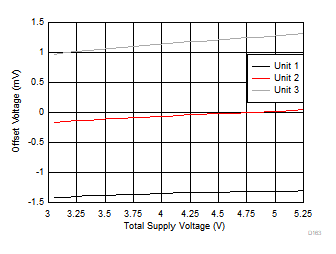
OPA858 Offset Voltage vs Supply Voltage
3 typical units
Figure 6-30 Offset Voltage vs Supply Voltage
OPA858 Offset Voltage vs Input Common-Mode Voltage
VS = 3.3 V 3 typical units
Figure 6-32 Offset Voltage vs Input Common-Mode Voltage
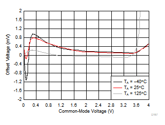
OPA858 Offset Voltage vs Input Common-Mode Voltage vs Ambient Temperature
 
Figure 6-34 Offset Voltage vs Input Common-Mode Voltage vs Ambient Temperature
OPA858 Offset Voltage vs Output Swing
VS = 5 V 3 typical units
Figure 6-36 Offset Voltage vs Output Swing
OPA858 Input
                        Bias Current vs Ambient Temperature
3 typical units
Figure 6-38 Input Bias Current vs Ambient Temperature
OPA858 Quiescent Current Distribution
µ = 20.35 mA σ = 0.2 mA 4555 units tested
Figure 6-40 Quiescent Current Distribution
OPA858 Input
                        Bias Current Distribution
µ = –0.1 pA σ = 0.39 pA 4555 units tested
Figure 6-42 Input Bias Current Distribution