SBOSA43A June 2021 – June 2025 TMCS1100-Q1
PRODUCTION DATA
- 1
- 1 Features
- 2 Applications
- 3 Description
- 4 Device Comparison
- 5 Pin Configuration and Functions
- 6 Specifications
- 7 Parameter Measurement Information
- 8 Detailed Description
- 9 Application and Implementation
- 10Device and Documentation Support
- 11Revision History
- 12Mechanical, Packaging, and Orderable Information
9.1.1 Total Error Calculation Examples
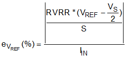
Total error can be calculated for any arbitrary device condition and current level. Error sources considered must include input-referred offset current, power-supply rejection, input common-mode rejection, sensitivity error, nonlinearity, VREF to VOUT gain error, and the error caused by any external fields. Compare each of these error sources in percentage terms, as some are significant drivers of error and some have inconsequential impact to current error. Offset (Equation 20), CMRR (Equation 22), PSRR (Equation 21), VREF gain error (Equation 23), and external field error (Equation 24) are all referred to the input, and so, are divided by the actual input current IIN to calculate percentage errors. For calculations of sensitivity error and nonlinearity error, the percentage limits explicitly specified in the Electrical Characteristics table can be used.


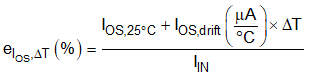
When calculating error contributions across temperature, only the input offset current and sensitivity error contributions vary significantly. For determining offset error over a given temperature range (ΔT), use Equation 25 to calculate total offset error current. Sensitivity error is specified for both –40°C to 85°C and –40°C to 125°C. The appropriate specification must be used based on application operating ambient temperature range.
To accurately calculate the total expected error of the device, the contributions from each of the individual components above must be understood in reference to operating conditions. To account for the individual error sources that are statistically uncorrelated, a root sum square (RSS) error calculation must be used to calculate total error. For the TMCS1100-Q1, only the input referred offset current (IOS), CMRR, and PSRR are statistically correlated. These error terms are lumped in an RSS calculation to reflect this nature, as shown in Equation 26 for room temperature and Equation 27 for across a given temperature range. The same methodology can be applied for calculating typical total error by using the appropriate error term specification.


The total error calculation has a strong dependence on the actual input current; therefore, always calculate total error across the dynamic range that is required. These curves asymptotically approach the sensitivity and nonlinearity error at high current levels, and approach infinity at low current levels due to offset error terms with input current in the denominator. Key figures of merit for any current-measurement system include the total error percentage at full-scale current, as well as the dynamic range of input current over which the error remains below some key level. Figure 9-1 illustrates the RSS maximum total error as a function of input current for a TMCS1100A2 at room temperature and across the full temperature range with VS of 5V.
 Figure 9-1 RSS Error vs. Input Current