SBOU244 June   2020 INA281


  1.   INA281EVM
    1.     Trademarks
    2. 1 General Texas Instruments High Voltage Evaluation (TI HV EVM) User Safety Guidelines
    3. 2 Overview
      1. 2.1 EVM Kit Contents
      2. 2.2 Related Documentation From Texas Instruments
    4. 3 Hardware
      1. 3.1 Features
    5. 4 Operation
      1. 4.1 Quick Start Setup
      2. 4.2 Measurements
    6. 5 EVM Components
      1. 5.1 R2_Xn, R3_Xn, R4_Xn, C2_Xn, C3_Xn
      2. 5.2 C1_Xn
      3. 5.3 R1_Xn
      4. 5.4 U1_Xn (INA281)
    7. 6 Schematic, PCB Layout, and Bill of Materials
      1. 6.1 Schematics
      2. 6.2 PCB Layout
      3. 6.3 Bill of Materials
        1. 6.3.1 Bill of Materials

Schematics

Figure 1 shows the schematic of the INA281EVM for all gain versions for the A pinout. The difference is noted on the reference designator ending in the gain option _An. Figure 2 shows the B1 gain panel and this is also a copy for all the other gain options with the reference designator ending with the gain option _Bn.
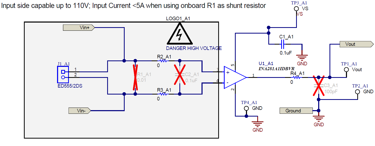
INA281 INA281EVM ina281evm-schematic-gain-a1-panel.pngFigure 1. INA281EVM Schematic: Gain A1 Panel
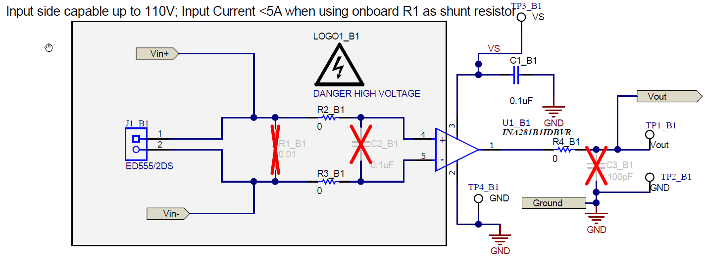
INA281 INA281EVM ina281evm-schematic-gain-b1-panel.pngFigure 2. INA281EVM Schematic: Gain B1 Panel