SBOU246 January   2022 TMP61 , TMP61-Q1 , TMP63 , TMP63-Q1 , TMP64 , TMP64-Q1


  1.   Trademarks
  2. 1Introduction
    1. 1.1 NTC Thermistor Versus TMP6 Linear Thermistor Family
    2. 1.2 NTC/Linear Thermistor TCR
    3. 1.3 NTC Versus Silicon-Based Linear Thermistor Trade-Offs
    4. 1.4 TMP6 Accuracy
  3. 2Typical NTC Thermistor Design Considerations
    1. 2.1 Voltage-Biased NTC Thermistor Network
    2. 2.2 Pinouts/Polarity
    3. 2.3 Converting NTC Thermistor Hardware Design to TMP6 Linear Thermistor Design
    4. 2.4 Simple Look-Up Table
  4. 3Software Changes
    1. 3.1 Firmware Design Considerations
    2. 3.2 Oversampling
    3. 3.3 Low-Pass Filtering in HW Versus SW
    4. 3.4 Calibration
  5. 4Design considerations for Full-Scale Range Voltage Output
    1. 4.1 Simple Current-Biased
    2. 4.2 Active Voltage-Biased
  6. 5Conclusion
  7. 6Additional Resources/Considerations
    1. 6.1 Constant-Current Source Design
    2. 6.2 TMP6 Thermistor Standard Component Footprints
    3. 6.3 Dual-Sourcing Approach for TMP6 and NTC Thermistors

Active Voltage-Biased

The hardware change for the active thermistor network involves a few more steps. Similar to the simple design above, the first hardware change is to swap the NTC and TMP61 thermistors, while RBIAS can remain as is.

Figure 4-4 TMP6 Linear Thermistor Schematic With Op Amp
Following the design steps of the guide, we end up with resistance values of RBIAS = 10 kΩ, R1 = 6.84 kΩ, R2 = 6.25 kΩ and R3 = 10 kΩ. The resulting V_OUT has range of 0.129 V to 4.86 V, which is within the linear operating range of the op amp and provides better resolution. These design decisions result in the voltage response shown in Figure 4-5 below.
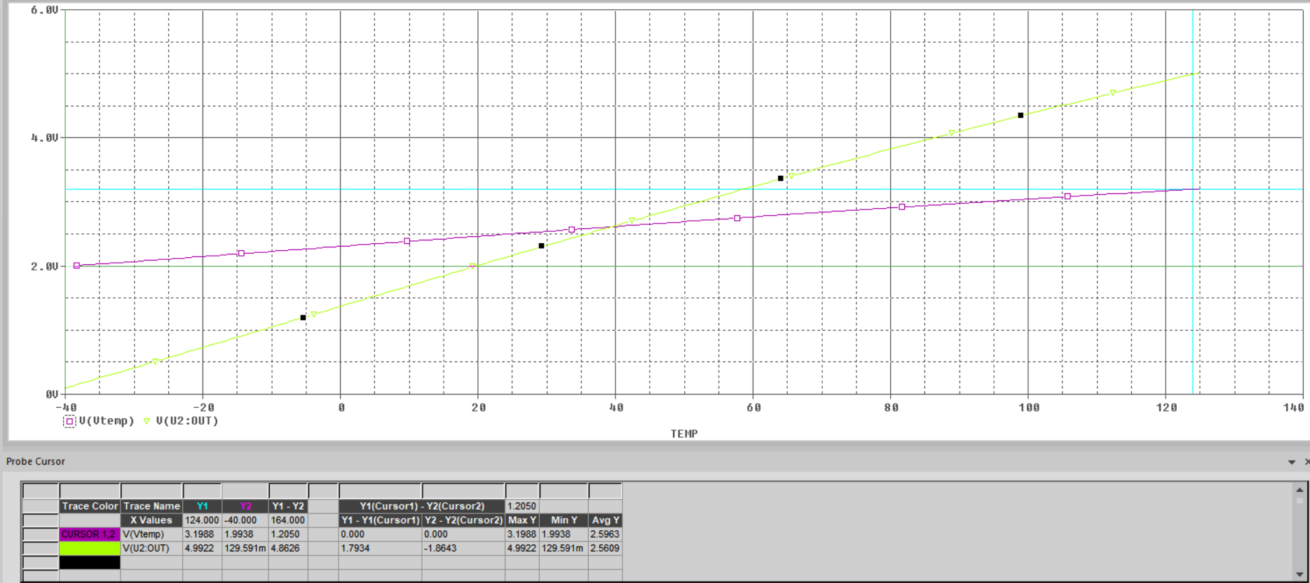
GUID-FC0615F2-BAEC-469A-A09F-2F5B3C6C62FB-low.pngFigure 4-5 TMP6 Linear Thermistor With Op Amp Voltage Response.