SDAA159 October 2025 XTR200
2.4 Simulations
The graphs in this section show the simulated performance of the circuit in various operating conditions. Figure 2-5 shows the current monitor output for increasing power supply output current with both sensitivities. The circuit simulates with excellent linearity across a wide range of currents.
 Figure 2-5 DC Transfer Characteristic of
Current Monitor Output
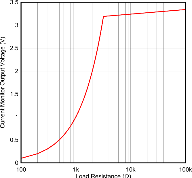
 Figure 2-6 Output Voltage for 1mA Monitor
Current and Increasing Load Resistance
Figure 2-6 Output Voltage for 1mA Monitor
Current and Increasing Load ResistanceFigure 2-6 illustrates the clamping functionality of the circuit. The plot shows the output voltage at the current monitor pin for a 1mA monitor current. The load resistance at the monitor pin is swept from 100Ω to 100kΩ. At 3.3kΩ of load resistance, the output voltage reaches 3.3V and the monitor circuit begins to clamp the output voltage. As the load resistance continues to increase, the output voltage remains relatively flat at 3.3V as the M-CRPS standard requires.
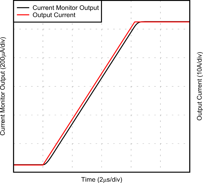
 Figure 2-7 Rising Edge Transient Response of
Current Monitor Output for 5% to 105% Load Step
 Figure 2-8 Falling Edge Transient Response of
Current Monitor Output for 105% to 5% Load Step
Figure 2-8 Falling Edge Transient Response of
Current Monitor Output for 105% to 5% Load StepFigure 2-7 and Figure 2-8 show the rising and falling transient response of the monitor circuit for a 5% to 105% (2.5A to 52.5A) load step, returning to 5%, with 8A/µs edge rates. The wide bandwidth of the XTR200 and the INA241A5 allows the monitor current to track the power supply output current with minimal delay or overshoot. The signal delay is far below the 20µs requirement of the standard.