SLAA558A November 2012 – October 2018 MSP430F5212 , MSP430F5214 , MSP430F5217 , MSP430F5219 , MSP430F5222 , MSP430F5224 , MSP430F5229 , MSP430F5252 , MSP430F5253 , MSP430F5254 , MSP430F5255 , MSP430F5256 , MSP430F5257 , MSP430F5258 , MSP430F5259
- Designing With MSP430F522x and MSP430F521x Devices
- Revision History
4 Split-Supply Power-Up or Power-Down Sequence
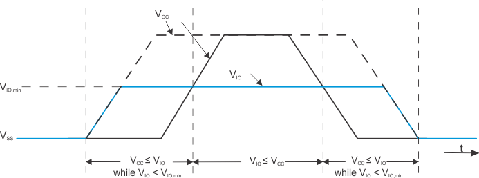
For split-supply I/O systems, it is required that the VIO ≥ VCC during the ramp up phase of VIO and VCC. During VCC and VIO power down, it is required that VIO ≥ VCC during the ramp down phase of VIO and VCC. Figure 2 is an excerpt from the data sheet.

The device supports continuous operation with VCC = VSS while VIO is fully within its specification. During this time, the general-purpose I/Os that reside on the VIO supply domain are configured as inputs and pulled down to VSS through their internal pulldown resistors. RST/NMI is high impedance. BSLEN is configured as an input and is pulled down to VSS through its internal pulldown resistor. When VCC reaches above the BOR threshold, the general-purpose I/Os become high-impedance inputs (no pullup or pulldown enabled), RST/NMI becomes an input pulled up to VIO through its internal pullup resistor, and BSLEN remains pulled down to VSS through its internal pulldown resistor.
Figure 2. VCC and VIO Power Sequencing