SLAAEB1 December 2023 MSPM0G1105 , MSPM0G1106 , MSPM0G1107 , MSPM0G1505 , MSPM0G1506 , MSPM0G1507 , MSPM0G3105 , MSPM0G3106 , MSPM0G3107 , MSPM0G3107-Q1 , MSPM0G3505 , MSPM0G3506 , MSPM0G3507 , MSPM0G3507-Q1 , MSPM0L1105 , MSPM0L1106 , MSPM0L1303 , MSPM0L1304 , MSPM0L1305 , MSPM0L1306 , MSPM0L1343 , MSPM0L1344 , MSPM0L1345 , MSPM0L1346
Description
The ADC to UART subsystem example demonstrates how to use the internal ADC to convert an analog signal into a digital representation and transfer the result through UART. The example configures the MCU to act as an external ADC and send raw ADC data through UART. Optionally the MCU can also preprocess the data then send it through I2C. Download the code for the ADC to UART example.
The following figure shows a block diagram of the system.
 Figure 1-1 Subsystem Functional Block Diagram
Required Peripherals
The application requires the internal ADC and 1 instance of UART
| Sub-block Functionality | Peripheral Used | Notes |
|---|---|---|
| Analog Signal Capture | ADC | Called ADC12_0_INST in code |
| Sending ADC data | UART | 2 UART transactions are done to send the full ADC data. |
Compatible Devices
Based on the requirements in the table above, the compatible devices are listed below. The corresponding EVM may be used for quick evaluation.
| Compatible Devices | EVM |
|---|---|
| MSPM0Lxxx | LP-MSPM0L1306 |
| MSPM0Gxxx | LP-MSPM0G3507 |
Design Steps
- Determine the configuration for the ADC including reference source, reference value, and sampling rate based on the expected analog input and design requirements.
- Configure the ADC in SysConfig based on requirements in the previous step.
- Configure the UART peripheral in SysConfig, setting the UART to the intended baud rate and other UART options for the intended communication.
- Write Application Code to transfer the ADC data from the memory registers to the UART. See the Software Flowchart for an overview or view the code directly.
Design Considerations
- Max Sampling Speed: The sampling speed of the ADC is based on input signal frequency, analog front end, filters or any other design parameters that affect sampling.
- ADC Reference: Choose the reference to align with the expected max input to utilize the full scale range of the ADC.
- Clock Settings: The clock source determines the total time for sample and conversion time. The clock divider in tandem with the SCOMP setting determine the total sampling time. SysConfig sets the appropriate SCOMP depending on the sampling time setting.
- UART configurations can be adjusted depending on the UART system, such as parity, baud rate, and more.
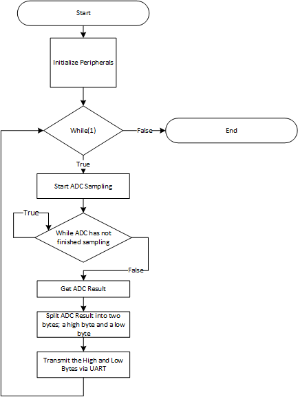
Software Flowchart
Application Code
The UART peripheral sends data in packets of 8 bits at a time. The ADC module stores the data into a 16-bit register. To transmit the data through the UART peripheral, the ADC data must be split into high and low bytes. The high byte contains the upper 8 bits while the low byte contains the lower 8 bits. Below is the code to split the ADC result and transmit the data through UART.
gADCResult = DL_ADC12_getMemResult(ADC12_0_INST, DL_ADC12_MEM_IDX_0);
uint8_t lowbyte  = (uint8_t)(gADCResult & 0xFF);
uint8_t highbyte = (uint8_t)((gADCResult >> 8) & 0xFF);
DL_UART_Main_transmitData(UART_0_INST, highbyte);
DL_UART_Main_transmitData(UART_0_INST, lowbyte);