SLAS916C November 2012 – November 2014 RF430CL330H
PRODUCTION DATA.
- 1Device Overview
- 2Revision History
- 3Terminal Configuration and Functions
-
4Specifications
- 4.1 Absolute Maximum Ratings
- 4.2 Handling Ratings
- 4.3 Recommended Operating Conditions
- 4.4 Recommended Operating Conditions, Resonant Circuit
- 4.5 Supply Currents
- 4.6 Digital Inputs
- 4.7 Digital Outputs
- 4.8 Thermal Characteristics
- 4.9 Serial Communication Protocol Timings
- 4.10 I2C Interface
- 4.11 SPI Interface
- 4.12 RF143B, Recommended Operating Conditions
- 4.13 RF143B, ISO14443B ASK Demodulator
- 4.14 RF143B, ISO14443B-Compliant Load Modulator
- 4.15 RF143B, Power Supply
- 5Detailed Description
- 6Device and Documentation Support
- 7Mechanical Packaging and Orderable Information
4 Specifications
4.1 Absolute Maximum Ratings(1)(2)
| MIN | MAX | UNIT | |
|---|---|---|---|
| Voltage applied at VCC referenced to VSS (VAMR) | -0.3 | 4.1 | V |
| Voltage applied at VANT referenced to VSS (VAMR) | -0.3 | 4.1 | V |
| Voltage applied to any pin (references to VSS) | -0.3 | VCC + 0.3 | V |
| Diode current at any device pin | ±2 | mA |
(1) Stresses beyond those listed under Absolute Maximum Ratings may cause permanent damage to the device. These are stress ratings only, and functional operation of the device at these or any other conditions beyond those indicated under Recommended Operating Conditions is not implied. Exposure to absolute-maximum-rated conditions for extended periods may affect device reliability.
(2) All voltages are referenced to VSS.
(3) For soldering during board manufacturing, it is required to follow the current JEDEC J-STD-020 specification with peak reflow temperatures not higher than classified on the device label on the shipping boxes or reels.
4.2 Handling Ratings
| MIN | MAX | UNIT | ||
|---|---|---|---|---|
| Tstg | Storage temperature range(3) | -40 | 125 | °C |
4.3 Recommended Operating Conditions
Typical values are specified at VCC = 3.3 V and TA = 25°C (unless otherwise noted)| MIN | NOM | MAX | UNIT | ||
|---|---|---|---|---|---|
| VCC | Supply voltage during program execution no RF field present | 3.0 | 3.3 | 3.6 | V |
| Supply voltage during program execution with RF field present | 2.0 | 3.3 | 3.6 | V | |
| VSS | Supply voltage (GND reference) | 0 | V | ||
| TA | Operating free-air temperature | -40 | 85 | °C | |
| C1 | Decoupling capacitor on VCC(1) | 0.1 | µF | ||
| C2 | Decoupling capacitor on VCC(1) | 1 | µF | ||
| CVCORE | Capacitor on VCORE(1) | 0.1 | 0.47 | 1 | µF |
(1) Low equivalent series resistance (ESR) capacitor
4.4 Recommended Operating Conditions, Resonant Circuit
| MIN | NOM | MAX | UNIT | ||
|---|---|---|---|---|---|
| fc | Carrier frequency | 13.56 | MHz | ||
| VANT_peak | Antenna input voltage | 3.6 | V | ||
| Z | Impedance of LC circuit | 6.5 | 15.5 | kΩ | |
| LRES | Coil inductance(2) | 2.66 | µH | ||
| CRES | Total resonance capacitance(2) CRES = CIN+CTune | 51.8 | pF | ||
| CTune | External resonance capacitance | CRES – CIN(1) | pF | ||
| QT | Tank quality factor | 30 |
(1) For CIN refer to Section 4.12.
(2) The coil inductance of the antenna LRES together with the external capacitance CTune plus the device internal capacitance CIN is a resonant circuit. The resonant frequency of this LC circuit must be close to the carrier frequency fc:
fRES = 1 / [2π(LRESCRES)1/2] = 1 / [2π(LRES(CIN + CTune))1/2] ≈ fc
fRES = 1 / [2π(LRESCRES)1/2] = 1 / [2π(LRES(CIN + CTune))1/2] ≈ fc
4.5 Supply Currents
over recommended ranges of supply voltage and operating free-air temperature (unless otherwise noted)| PARAMETER | TEST CONDITIONS | VCC | MIN | TYP | MAX | UNIT | |
|---|---|---|---|---|---|---|---|
| ICC(SPI) | SPI, fSCK,MAX, SO = Open, Writing into NDEF memory | 3.3 V | 250 | µA | |||
| ICC(I2C) | I2C, 400 kHz, Writing into NDEF memory | 3.3 V | 250 | µA | |||
| ICC(RF enabled) | RF enabled, no RF field present | 3.3 V | 40 | µA | |||
| ICC(Inactive) | Standby enable = 0, RF disabled, no serial communication | 3.3 V | 15 | µA | |||
| ICC(Standby) | Standby enable = 1, RF disabled, no serial communication | 3.3 V | 10 | 45 | µA | ||
| ΔICC(StrongRF) | Additional current consumption with strong RF field present | 3.0 V to 3.6 V | 160 | µA | |||
| ICC(RF,lowVCC) | Current drawn from VCC < 3.0 V with RF field present (passive operation) | 2.0 V to 3.0 V | 0 | µA | |||
4.6 Digital Inputs
over recommended ranges of supply voltage and operating free-air temperature (unless otherwise noted)| PARAMETER | TEST CONDITIONS | VCC | MIN | TYP | MAX | UNIT | |
|---|---|---|---|---|---|---|---|
| VIL | Low-level input voltage | 0.3× VCC | V | ||||
| VIH | High-level input voltage | 0.7× VCC | V | ||||
| VHYS | Input hysteresis | 0.1× VCC | V | ||||
| IL | High-impedance leakage current | 3.3 V | -50 | 50 | nA | ||
| RPU(RST) | Integrated RST pullup resistor | 20 | 35 | 50 | kΩ | ||
| RPU(CS) | Integrated SCMS/CS pullup resistor (only active during initialization) | 20 | 35 | 50 | kΩ | ||
4.7 Digital Outputs
over recommended ranges of supply voltage and operating free-air temperature (unless otherwise noted)| PARAMETER | TEST CONDITIONS | VCC | MIN | TYP | MAX | UNIT | |
|---|---|---|---|---|---|---|---|
| VOL | Output low voltage | IOL = 3 mA | 3 V | 0.4 | V | ||
| 3.3 V | 0.4 | ||||||
| 3.6 V | 0.4 | ||||||
| VOH | Output high voltage | IOH = -3 mA | 3 V | 2.6 | V | ||
| 3.3 V | 2.9 | ||||||
| 3.6 V | 3.2 | ||||||
4.8 Thermal Characteristics
over operating free-air temperature range (unless otherwise noted)| PARAMETER | VALUE | UNIT | ||
|---|---|---|---|---|
| θJA | Junction-to-ambient thermal resistance, still air(1) | TSSOP-14 (PW) | 116.0 | °C/W |
| θJC(TOP) | Junction-to-case (top) thermal resistance(2) | 45.1 | °C/W | |
| θJB | Junction-to-board thermal resistance(3) | 57.6 | °C/W | |
| ΨJB | Junction-to-board thermal characterization parameter | 57.0 | °C/W | |
| ΨJT | Junction-to-top thermal characterization parameter | 4.6 | °C/W | |
| θJA | Junction-to-ambient thermal resistance, still air(1) | VQFN-16 (RGT) | 48.8 | °C/W |
| θJC(TOP) | Junction-to-case (top) thermal resistance(2) | 60.8 | °C/W | |
| θJB | Junction-to-board thermal resistance(3) | 21.9 | °C/W | |
| ΨJB | Junction-to-board thermal characterization parameter | 21.9 | °C/W | |
| ΨJT | Junction-to-top thermal characterization parameter | 1.5 | °C/W | |
| θJC(BOT) | Junction-to-case (bottom) thermal resistance(4) | 7.1 | °C/W | |
(1) The junction-to-ambient thermal resistance under natural convection is obtained in a simulation on a JEDEC-standard, High-K board, as specified in JESD51-7, in an environment described in JESD51-2a.
(2) The junction-to-case (top) thermal resistance is obtained by simulating a cold plate test on the package top. No specific JEDEC standard test exists, but a close description can be found in the ANSI SEMI standard G30-88.
(3) The junction-to-board thermal resistance is obtained by simulating in an environment with a ring cold plate fixture to control the PCB temperature, as described in JESD51-8.
(4) The junction-to-case (bottom) thermal resistance is obtained by simulating a cold plate test on the exposed (power) pad. No specific JEDEC standard test exists, but a close description can be found in the ANSI SEMI standard G30-88.
4.9 Serial Communication Protocol Timings
over recommended ranges of supply voltage and operating free-air temperature (unless otherwise noted)| PARAMETER | MIN | TYP | MAX | UNIT | |
|---|---|---|---|---|---|
| tSPIvsI2C | Time after power-up or reset until SCMS/CS is sampled for SPI or I2C decision(1) | 1 | 10 | ms | |
| tReady | Time after power-up or reset until device is ready to communicate using SPI or I2C(2) | 20 | ms | ||
(1) The SCMS/CS pin is sampled after tSPIvsI2C(MIN) at the earliest and after tSPIvsI2C(MAX) at the latest.
(2) The device is ready to communicate after tReady(MAX) at the latest.
4.10 I2C Interface
over recommended ranges of supply voltage and operating free-air temperature (unless otherwise noted) (see Figure 4-1)| PARAMETER | TEST CONDITIONS | VCC | MIN | TYP | MAX | UNIT | |
|---|---|---|---|---|---|---|---|
| fSCL | SCL clock frequency (with Master supporting clock stretching according to I2C standard, or when the device is not being addressed) | 3.3 V | 0 | 400 | kHz | ||
| SCL clock frequency (device being addressed by Master not supporting clock stretching) | write | 3.3 V | 0 | 120 | kHz | ||
| read | 3.3 V | 0 | 100 | kHz | |||
| tHD,STA | Hold time (repeated) START | fSCL ≤ 100 kHz | 3.3 V | 4 | µs | ||
| fSCL > 100 kHz | 0.6 | ||||||
| tSU,STA | Setup time for a repeated START | fSCL ≤ 100 kHz | 3.3 V | 4.7 | µs | ||
| fSCL > 100 kHz | 0.6 | ||||||
| tHD,DAT | Data hold time | 3.3 V | 0 | ns | |||
| tSU,DAT | Data setup time | 3.3 V | 250 | ns | |||
| tSU,STO | Setup time for STOP | 3.3 V | 4 | µs | |||
| tSP | Pulse duration of spikes suppressed by input filter | 3.3 V | 6.25 | 75 | ns | ||
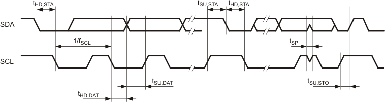 Figure 4-1 I2C Mode Timing
4.11 SPI Interface
over recommended ranges of supply voltage and operating free-air temperature (unless otherwise noted)| PARAMETER | TEST CONDITIONS | VCC | MIN | TYP | MAX | UNIT | |
|---|---|---|---|---|---|---|---|
| fSCK | SCK clock frequency | write | 3.3 V | 0 | 100 | kHz | |
| read | 3.3 V | 0 | 110 | kHz | |||
| tHIGH,CS | CS high time | 3.3 V | 50 | µs | |||
| tSU,CS | CS setup time | 3.3 V | 25 | µs | |||
| tHD,CS | CS hold time | 3.3 V | 100 | ns | |||
| tHIGH | SCK high time | 3.3 V | 100 | ns | |||
| tLOW | SCK low time | 3.3 V | 100 | ns | |||
| tSU,SI | Data In (SI) setup time | 3.3 V | 50 | ns | |||
| tHD,SI | Data In (SI) hold time | 3.3 V | 50 | ns | |||
| tVALID,SO | Output (SO) valid | 3.3 V | 0 | 50 | ns | ||
| tHOLD,SO | Output (SO) hold time | 3.3 V | 0 | ns | |||
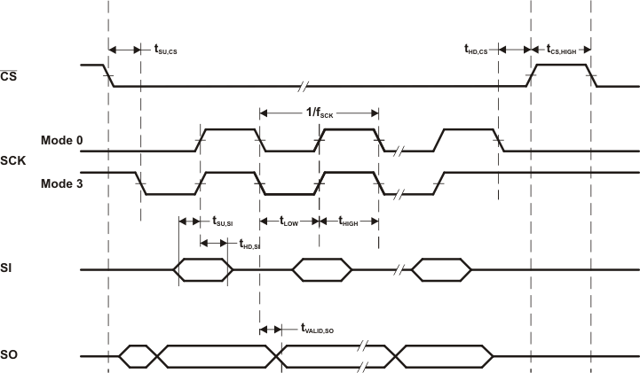 Figure 4-2 SPI Mode Timing
4.12 RF143B, Recommended Operating Conditions
over recommended ranges of supply voltage and operating free-air temperature (unless otherwise noted)| PARAMETER | TEST CONDITIONS | MIN | TYP | MAX | UNIT | |
|---|---|---|---|---|---|---|
| VDDH | Antenna rectified voltage | Peak voltage limited by antenna limiter | 3.0 | 3.3 | 3.6 | V |
| IDDH | Antenna load current | RMS, without limiter current | 100 | µA | ||
| CIN | Input capacitance | ANT1 to ANT2, 2 V RMS | 31.5 | 35 | 38.5 | pF |
4.13 RF143B, ISO14443B ASK Demodulator
over recommended ranges of supply voltage and operating free-air temperature (unless otherwise noted)| PARAMETER | MIN | TYP | MAX | UNIT | |
|---|---|---|---|---|---|
| DR10 | Input signal data rate 10% downlink modulation, 7% to 30% ASK, ISO1443B | 106 | 848 | kbps | |
| m10 | Modulation depth 10%, tested as defined in ISO10373 | 7 | 30 | % | |
4.14 RF143B, ISO14443B-Compliant Load Modulator
over recommended ranges of supply voltage and operating free-air temperature (unless otherwise noted)| PARAMETER | MIN | TYP | MAX | UNIT | |
|---|---|---|---|---|---|
| fPICC | Uplink subcarrier modulation frequency | 0.2 | 1 | MHz | |
| VA_MOD | Modulated antenna voltage, VA_unmod = 2.3 V | 0.5 | V | ||
| VSUB14 | Uplink modulation subcarrier level, ISO14443B: H = 1.5 to 7.5 A/m | 22/H0.5 | mV | ||
4.15 RF143B, Power Supply
over recommended ranges of supply voltage and operating free-air temperature (unless otherwise noted)| PARAMETER | TEST CONDITIONS | MIN | TYP | MAX | UNIT | |
|---|---|---|---|---|---|---|
| VLIM | Limiter clamping voltage | ILIM ≤ 70 mA RMS, f = 13.56 MHz | 3.0 | 3.6 | Vpk | |
| ILIM,MAX | Maximum limiter current | 70 | mA | |||