SLAS989D January 2014 – October 2017 ADC12J4000
PRODUCTION DATA.
- 1 Features
- 2 Applications
- 3 Description
- 4 Revision History
- 5 Pin Configuration and Functions
- 6 Specifications
-
7 Detailed Description
- 7.1 Overview
- 7.2 Functional Block Diagram
- 7.3
Feature Description
- 7.3.1 Signal Acquisition
- 7.3.2 The Analog Inputs
- 7.3.3 Clocking
- 7.3.4 Over-Range Function
- 7.3.5 ADC Core Features
- 7.3.6
Digital Down Converter (DDC)
- 7.3.6.1 NCO/Mixer
- 7.3.6.2 NCO Settings
- 7.3.6.3 Decimation Filters
- 7.3.6.4 DDC Output Data
- 7.3.6.5 Decimation Settings
- 7.3.7
Data Outputs
- 7.3.7.1 The Digital Outputs
- 7.3.7.2
JESD204B Interface Features and Settings
- 7.3.7.2.1 Scrambler Enable
- 7.3.7.2.2 Frames Per Multi-Frame (K-1)
- 7.3.7.2.3 DDR
- 7.3.7.2.4 JESD Enable
- 7.3.7.2.5 JESD Test Modes
- 7.3.7.2.6 Configurable Pre-Emphasis
- 7.3.7.2.7 Serial Output-Data Formatting
- 7.3.7.2.8 JESD204B Synchronization Features
- 7.3.7.2.9 SYSREF
- 7.3.7.2.10 SYNC~
- 7.3.7.2.11 Time Stamp
- 7.3.7.2.12 Code-Group Synchronization
- 7.3.7.2.13 Multiple ADC Synchronization
- 7.4 Device Functional Modes
- 7.5 Programming
- 7.6
Register Map
- 7.6.1 Memory Map
- 7.6.2
Register Descriptions
- 7.6.2.1
Standard SPI-3.0 (0x000 to 0x00F)
- 7.6.2.1.1 Configuration A Register (address = 0x000) [reset = 0x3C]
- 7.6.2.1.2 Configuration B Register (address = 0x001) [reset = 0x00]
- 7.6.2.1.3 Device Configuration Register (address = 0x002) [reset = 0x00]
- 7.6.2.1.4 Chip Type Register (address = 0x003) [reset = 0x03]
- 7.6.2.1.5 Chip Version Register (address = 0x006) [reset = 0x13]
- 7.6.2.1.6 Vendor Identification Register (address = 0x00C to 0x00D) [reset = 0x0451]
- 7.6.2.2 User SPI Configuration (0x010 to 0x01F)
- 7.6.2.3
General Analog, Bias, Band Gap, and Track and Hold (0x020 to 0x02F)
- 7.6.2.3.1 Power-On Reset Register (address = 0x021) [reset = 0x00]
- 7.6.2.3.2 I/O Gain 0 Register (address = 0x022) [reset = 0x40]
- 7.6.2.3.3 IO_GAIN_1 Register (address = 0x023) [reset = 0x00]
- 7.6.2.3.4 I/O Offset 0 Register (address = 0x025) [reset = 0x40]
- 7.6.2.3.5 I/O Offset 1 Register (address = 0x026) [reset = 0x00]
- 7.6.2.4
Clock (0x030 to 0x03F)
- 7.6.2.4.1 Clock Generator Control 0 Register (address = 0x030) [reset = 0xC0]
- 7.6.2.4.2 Clock Generator Status Register (address = 0x031) [reset = 0x07]
- 7.6.2.4.3 Clock Generator Control 2 Register (address = 0x032) [reset = 0x80]
- 7.6.2.4.4 Analog Miscellaneous Register (address = 0x033) [reset = 0xC3]
- 7.6.2.4.5 Input Clamp Enable Register (address = 0x034) [reset = 0x2F]
- 7.6.2.5 Serializer (0x040 to 0x04F)
- 7.6.2.6
ADC Calibration (0x050 to 0x1FF)
- 7.6.2.6.1 Calibration Configuration 0 Register (address = 0x050) [reset = 0x06]
- 7.6.2.6.2 Calibration Configuration 1 Register (address = 0x051) [reset = 0xF4]
- 7.6.2.6.3 Calibration Background Control Register (address = 0x057) [reset = 0x10]
- 7.6.2.6.4 ADC Pattern and Over-Range Enable Register (address = 0x058) [reset = 0x00]
- 7.6.2.6.5 Calibration Vectors Register (address = 0x05A) [reset = 0x00]
- 7.6.2.6.6 Calibration Status Register (address = 0x05B) [reset = undefined]
- 7.6.2.6.7 Timing Calibration Register (address = 0x066) [reset = 0x02]
- 7.6.2.7
Digital Down Converter and JESD204B (0x200-0x27F)
- 7.6.2.7.1 Digital Down-Converter (DDC) Control Register (address = 0x200) [reset = 0x10]
- 7.6.2.7.2 JESD204B Control 1 Register (address = 0x201) [reset = 0x0F]
- 7.6.2.7.3 JESD204B Control 2 Register (address = 0x202) [reset = 0x00]
- 7.6.2.7.4 JESD204B Device ID (DID) Register (address = 0x203) [reset = 0x00]
- 7.6.2.7.5 JESD204B Control 3 Register (address = 0x204) [reset = 0x00]
- 7.6.2.7.6 JESD204B and System Status Register (address = 0x205) [reset = Undefined]
- 7.6.2.7.7 Overrange Threshold 0 Register (address = 0x206) [reset = 0xF2]
- 7.6.2.7.8 Overrange Threshold 1 Register (address = 0x207) [reset = 0xAB]
- 7.6.2.7.9 Overrange Period Register (address = 0x208) [reset = 0x00]
- 7.6.2.7.10 DDC Configuration Preset Mode Register (address = 0x20C) [reset = 0x00]
- 7.6.2.7.11 DDC Configuration Preset Select Register (address = 0x20D) [reset = 0x00]
- 7.6.2.7.12 Rational NCO Reference Divisor Register (address = 0x20E to 0x20F) [reset = 0x0000]
- 7.6.2.7.13 NCO Frequency (Preset x) Register (address = see ) [reset = see ]
- 7.6.2.7.14 NCO Phase (Preset x) Register (address = see ) [reset = see ]
- 7.6.2.7.15 DDC Delay (Preset x) Register (address = see ) [reset = see ]
- 7.6.2.1
Standard SPI-3.0 (0x000 to 0x00F)
- 8 Application and Implementation
- 9 Power Supply Recommendations
- 10Layout
- 11Device and Documentation Support
- 12Mechanical, Packaging, and Orderable Information
10 Layout
10.1 Layout Guidelines
Proper grounding and proper routing of all signals is essential to ensure accurate conversion. Each ground layer should be a single unified ground plane, rather than splitting the ground planes into analog and digital areas.
Because digital switching transients are composed largely of high frequency components, the skin effect dictates that the total ground-plane copper weight has little effect upon the logic-generated noise. Total surface area is more important than the total ground-plane volume. Coupling between the typically-noisy digital circuitry and the sensitive analog circuitry can lead to poor performance that can be impossible to isolate and remedy. The solution is to keep the analog circuitry well separated from the digital circuitry.
High-power digital components must not be located on or near any linear component or power-supply trace or plane that services analog or mixed-signal components because the resulting common return current path could cause fluctuation in the analog input ground return of the ADC which causes excessive noise in the conversion result.
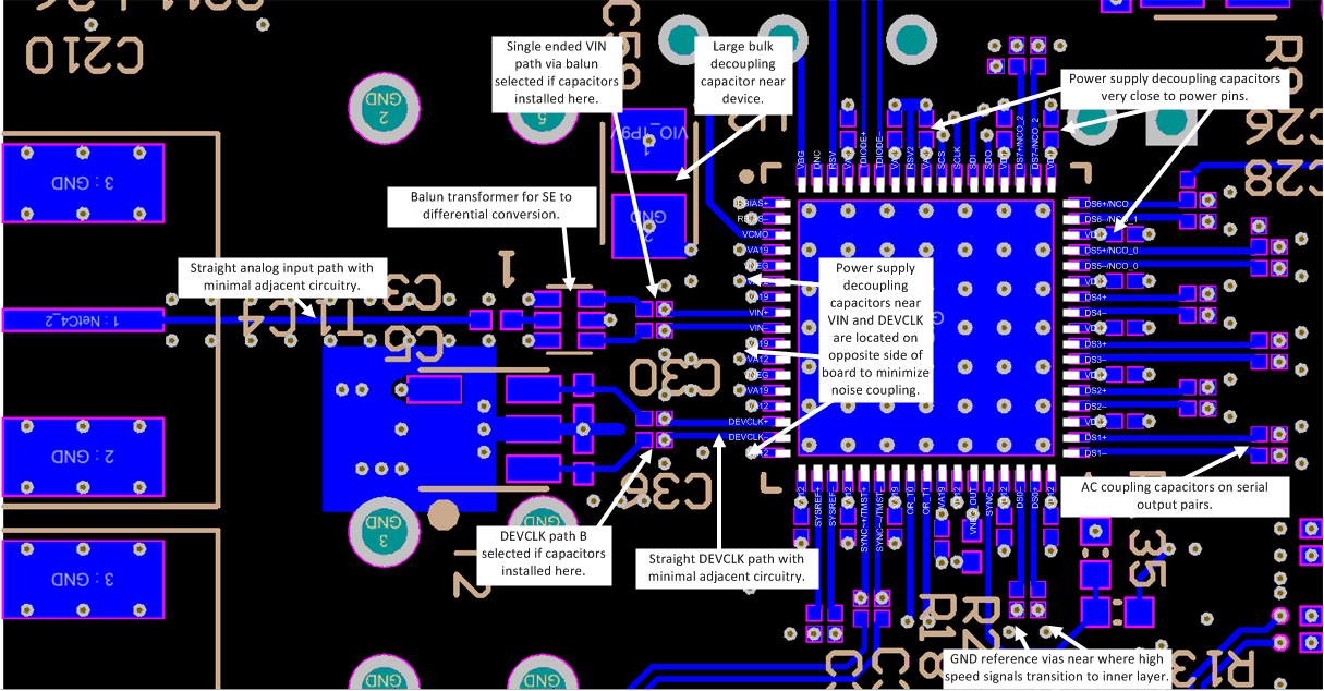
In general, assume that analog and digital lines must cross each other at 90° to avoid digital noise into the analog path. In high frequency systems, however, avoid crossing analog and digital lines altogether. The input clock lines must be isolated from all other lines, both analog and digital. The generally-accepted 90° crossing must be avoided because even a same amount of coupling causes problems at high frequencies. Best performance at high frequencies is obtained with a straight signal path.
Coupling onto or between the clock and input signal paths must be avoided using any isolation techniques available including distance isolation, orientation planning to prevent field coupling of components like inductors and transformers, and providing well coupled reference planes. Via stitching around the clock signal path and the input analog signal path provides a quiet ground reference for the critical signal paths and reduces noise coupling onto these paths. Sensitive signal traces must not cross other signal traces or power routing on adjacent PCB layers, rather a ground plane must separate the traces. If necessary, the traces should cross at 90° angles to minimize crosstalk.
Isolation of the analog input is important because of the low-level drive required of the ADC12J4000 device. Quality analog input signal and clock signal path layout is required for full dynamic performance. Symmetry of the differential signal paths and discrete components in the path is mandatory and symmetrical shunt-oriented components should have a common grounding via. The high frequency requirements of the input and clock signal paths necessitate using differential routing with controlled impedances and minimizing signal path stubs (including vias) when possible.
Layout of the high-speed serial-data lines is of particular importance. These traces must be routed as tightly coupled 100-Ω differential pairs, with minimal vias. When vias must be used, care must be taken to implement control-impedance vias (that is, 50-Ω) with adjacent ground vias for image current control.
10.2 Layout Example
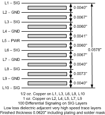
The following examples show layout-example plots (top and bottom layers only). Figure 102 shows a typical stackup for a 10 layer board.
 Figure 100. ADC12J4000 Layout Example 1 — Top Side
 Figure 101. ADC12J4000 Layout Example 2 — Bottom Side
 Figure 102. ADC12J4000 Typical Stackup — 10 Layer Board
10.3 Thermal Management
The ADC12J4000 device is capable of impressive speeds and performance at low power levels for speed. However, the power consumption is still high enough to require attention to thermal management. The VQFN package has a primary-heat transfer path through the center pad on the bottom of the package. The thermal resistance of this path is provided as RθJCbot.
For reliability reasons, the die temperature must be kept to a maximum of 135°C which is the ambient temperature (TA) plus the ADC power consumption multiplied by the net junction-to-ambient thermal resistance (RθJA). Maintaining this temperature is not a problem if the ambient temperature is kept to a maximum of 85°C as specified in the Recommended Operating Conditions table and the center ground pad on the bottom of the package is thermally connected to a large-enough copper area of the PC board.
The package of the ADC12J4000 device has a center pad that provides the primary heat-removal path as well as excellent electrical grounding to the PCB. Recommended land pattern and solder paste examples are provided in the Mechanical, Packaging, and Orderable Information section. The center-pad vias shown must be connected to internal ground planes to remove the maximum amount of heat from the package, as well as to ensure best product parametric performance.
If needed to further reduce junction temperature, TI recommends to build a simple heat sink into the PCB which occurs by including a copper area of about 1 to 2 cm2 on the opposite side of the PCB. This copper area can be plated or solder-coated to prevent corrosion, but should not have a conformal coating which would provide thermal insulation. Thermal vias will be used to connect these top and bottom copper areas and internal ground planes. These thermal vias act as heat pipes to carry the thermal energy from the device side of the board to the opposite side of the board where the heat can be more effectively dissipated.