SLAS989D January 2014 – October 2017 ADC12J4000
PRODUCTION DATA.
- 1 Features
- 2 Applications
- 3 Description
- 4 Revision History
- 5 Pin Configuration and Functions
- 6 Specifications
-
7 Detailed Description
- 7.1 Overview
- 7.2 Functional Block Diagram
- 7.3
Feature Description
- 7.3.1 Signal Acquisition
- 7.3.2 The Analog Inputs
- 7.3.3 Clocking
- 7.3.4 Over-Range Function
- 7.3.5 ADC Core Features
- 7.3.6
Digital Down Converter (DDC)
- 7.3.6.1 NCO/Mixer
- 7.3.6.2 NCO Settings
- 7.3.6.3 Decimation Filters
- 7.3.6.4 DDC Output Data
- 7.3.6.5 Decimation Settings
- 7.3.7
Data Outputs
- 7.3.7.1 The Digital Outputs
- 7.3.7.2
JESD204B Interface Features and Settings
- 7.3.7.2.1 Scrambler Enable
- 7.3.7.2.2 Frames Per Multi-Frame (K-1)
- 7.3.7.2.3 DDR
- 7.3.7.2.4 JESD Enable
- 7.3.7.2.5 JESD Test Modes
- 7.3.7.2.6 Configurable Pre-Emphasis
- 7.3.7.2.7 Serial Output-Data Formatting
- 7.3.7.2.8 JESD204B Synchronization Features
- 7.3.7.2.9 SYSREF
- 7.3.7.2.10 SYNC~
- 7.3.7.2.11 Time Stamp
- 7.3.7.2.12 Code-Group Synchronization
- 7.3.7.2.13 Multiple ADC Synchronization
- 7.4 Device Functional Modes
- 7.5 Programming
- 7.6
Register Map
- 7.6.1 Memory Map
- 7.6.2
Register Descriptions
- 7.6.2.1
Standard SPI-3.0 (0x000 to 0x00F)
- 7.6.2.1.1 Configuration A Register (address = 0x000) [reset = 0x3C]
- 7.6.2.1.2 Configuration B Register (address = 0x001) [reset = 0x00]
- 7.6.2.1.3 Device Configuration Register (address = 0x002) [reset = 0x00]
- 7.6.2.1.4 Chip Type Register (address = 0x003) [reset = 0x03]
- 7.6.2.1.5 Chip Version Register (address = 0x006) [reset = 0x13]
- 7.6.2.1.6 Vendor Identification Register (address = 0x00C to 0x00D) [reset = 0x0451]
- 7.6.2.2 User SPI Configuration (0x010 to 0x01F)
- 7.6.2.3
General Analog, Bias, Band Gap, and Track and Hold (0x020 to 0x02F)
- 7.6.2.3.1 Power-On Reset Register (address = 0x021) [reset = 0x00]
- 7.6.2.3.2 I/O Gain 0 Register (address = 0x022) [reset = 0x40]
- 7.6.2.3.3 IO_GAIN_1 Register (address = 0x023) [reset = 0x00]
- 7.6.2.3.4 I/O Offset 0 Register (address = 0x025) [reset = 0x40]
- 7.6.2.3.5 I/O Offset 1 Register (address = 0x026) [reset = 0x00]
- 7.6.2.4
Clock (0x030 to 0x03F)
- 7.6.2.4.1 Clock Generator Control 0 Register (address = 0x030) [reset = 0xC0]
- 7.6.2.4.2 Clock Generator Status Register (address = 0x031) [reset = 0x07]
- 7.6.2.4.3 Clock Generator Control 2 Register (address = 0x032) [reset = 0x80]
- 7.6.2.4.4 Analog Miscellaneous Register (address = 0x033) [reset = 0xC3]
- 7.6.2.4.5 Input Clamp Enable Register (address = 0x034) [reset = 0x2F]
- 7.6.2.5 Serializer (0x040 to 0x04F)
- 7.6.2.6
ADC Calibration (0x050 to 0x1FF)
- 7.6.2.6.1 Calibration Configuration 0 Register (address = 0x050) [reset = 0x06]
- 7.6.2.6.2 Calibration Configuration 1 Register (address = 0x051) [reset = 0xF4]
- 7.6.2.6.3 Calibration Background Control Register (address = 0x057) [reset = 0x10]
- 7.6.2.6.4 ADC Pattern and Over-Range Enable Register (address = 0x058) [reset = 0x00]
- 7.6.2.6.5 Calibration Vectors Register (address = 0x05A) [reset = 0x00]
- 7.6.2.6.6 Calibration Status Register (address = 0x05B) [reset = undefined]
- 7.6.2.6.7 Timing Calibration Register (address = 0x066) [reset = 0x02]
- 7.6.2.7
Digital Down Converter and JESD204B (0x200-0x27F)
- 7.6.2.7.1 Digital Down-Converter (DDC) Control Register (address = 0x200) [reset = 0x10]
- 7.6.2.7.2 JESD204B Control 1 Register (address = 0x201) [reset = 0x0F]
- 7.6.2.7.3 JESD204B Control 2 Register (address = 0x202) [reset = 0x00]
- 7.6.2.7.4 JESD204B Device ID (DID) Register (address = 0x203) [reset = 0x00]
- 7.6.2.7.5 JESD204B Control 3 Register (address = 0x204) [reset = 0x00]
- 7.6.2.7.6 JESD204B and System Status Register (address = 0x205) [reset = Undefined]
- 7.6.2.7.7 Overrange Threshold 0 Register (address = 0x206) [reset = 0xF2]
- 7.6.2.7.8 Overrange Threshold 1 Register (address = 0x207) [reset = 0xAB]
- 7.6.2.7.9 Overrange Period Register (address = 0x208) [reset = 0x00]
- 7.6.2.7.10 DDC Configuration Preset Mode Register (address = 0x20C) [reset = 0x00]
- 7.6.2.7.11 DDC Configuration Preset Select Register (address = 0x20D) [reset = 0x00]
- 7.6.2.7.12 Rational NCO Reference Divisor Register (address = 0x20E to 0x20F) [reset = 0x0000]
- 7.6.2.7.13 NCO Frequency (Preset x) Register (address = see ) [reset = see ]
- 7.6.2.7.14 NCO Phase (Preset x) Register (address = see ) [reset = see ]
- 7.6.2.7.15 DDC Delay (Preset x) Register (address = see ) [reset = see ]
- 7.6.2.1
Standard SPI-3.0 (0x000 to 0x00F)
- 8 Application and Implementation
- 9 Power Supply Recommendations
- 10Layout
- 11Device and Documentation Support
- 12Mechanical, Packaging, and Orderable Information
6 Specifications
6.1 Absolute Maximum Ratings
The soldering process must comply with TI's Reflow Temperature Profile specifications. Refer to www.ti.com/packaging.(5)(1)(3)| MIN | MAX | UNIT | |||
|---|---|---|---|---|---|
| Supply voltage | 1.2-V supply | VA12, VD12 | 1.4 | V | |
| 1.9-V supply | VA19 | 2.2 | |||
| 1.2-V supply difference between VA12 and VD12 | –200 | 200 | mV | ||
| Voltage | On any input pin (except VIN+ or VIN–) | –0.15 | V(VA19) + 0.15 | V | |
| On VIN+ or VIN– | 0 | 2 | |||
| Voltage difference | |(VIN+) – (VIN–)|(2) | 2 | V | ||
| |(DEVCLK+) – (DEVCLK–)| | 2 | ||||
| |(SYSREF+) – (SYSREF–)| | 2 | ||||
| |(~SYNC+) – (~SYNC–)| | 1 | ||||
| RF input power, PI | On VIN+, VIN–, with proper input common mode maintained. FIN ≥ 3 GHz, Z(SOURCE) = 100 Ω, Input_Clamp_EN = 0 or 1 | 11.07 | dBm | ||
| On VIN+, VIN–, with proper input common mode maintained. FIN = 1 GHz, Z(SOURCE) = 100 Ω, Input_Clamp_EN = 1 | 14.95 | ||||
| On VIN+, VIN–, with proper input common mode maintained. FIN ≤ 100 MHz, Z(SOURCE) = 100 Ω, Input_Clamp_EN = 1 | 20.97 | ||||
| Input current | At any pin other than VIN+ or VIN–(4) | –25 | 25 | mA | |
| VIN+ or VIN– | –50 | 50 | mA DC | ||
| Package(4) (sum of absolute value of all currents forced in or out, not including power supply current) | 100 | mA | |||
| Junction temperature, TJ | Power applied. Verified by High Temperature Operation Life testing to 1000 hours. | –40 | 150 | °C | |
| Storage temperature, Tstg | –65 | 150 | °C | ||
(1) Stresses beyond those listed under Absolute Maximum Ratings may cause permanent damage to the device. These are stress ratings only, and functional operation of the device at these or any other conditions beyond those indicated under Recommended Operating Conditions is not implied. Exposure to absolute-maximum-rated conditions for extended periods may affect device reliability.
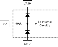
(2) The analog inputs are protected as in the following circuit. Input-voltage magnitudes beyond the Absolute Maximum Ratings may damage this device.

(3) If Military/Aerospace specified devices are required, please contact the Texas Instruments Sales Office/Distributors for availability and specifications.
(4) When the input voltage at any pin (other than VIN+ or VIN–) exceeds the power supply limits (that is, less than GND or greater than VA19), the current at that pin must be limited to 25 mA. The 100-mA maximum package input current rating limits the number of pins that can safely exceed the power supplies. This limit is not placed upon the power pins or thermal pad (GND).
(5) Reflow temperature profiles are different for lead-free and non-lead-free packages.
6.2 ESD Ratings
| VALUE | UNIT | |||
|---|---|---|---|---|
| V(ESD) | Electrostatic discharge | Human body model (HBM), per ANSI/ESDA/JEDEC JS-001, all pins(1) | ±2000 | V |
| Charged device model (CDM), per JEDEC specification JESD22-C101, all pins(2) | ±500 | |||
(1) JEDEC document JEP155 states that 500-V HBM allows safe manufacturing with a standard ESD control process.
(2) JEDEC document JEP157 states that 250-V CDM allows safe manufacturing with a standard ESD control process.
6.3 Recommended Operating Conditions
All voltages are measured with respect to GND = 0 V, unless otherwise specified.6.4 Thermal Information
| THERMAL METRIC(1) | ADC12J4000 | UNIT | |
|---|---|---|---|
| NKE (VQFN) | |||
| 68 PINS | |||
| RθJA | Thermal resistance, junction-to-ambient | 19.8 | °C/W |
| RθJCbot | Thermal resistance, junction-to-case (bottom) | 2.7 | °C/W |
| ψJB | Characterization parameter, junction-to-board | 9.1 | °C/W |
(1) For more information about traditional and new thermal metrics, see the Semiconductor and IC Package Thermal Metrics application report.
6.5 Electrical Characteristics
Unless otherwise noted, these specifications apply for V(VA12) = V(VD12) = 1.2 V, V(VA19) = 1.9 V, VIN full scale range at default setting (725 mVPP), VIN = –1 dBFS, differential AC-coupled sinewave input clock, ƒ(DEVCLK) = 4 GHz at 0.5 VPP with 50% duty cycle, R(RBIAS) = 3.3 kΩ ±0.1%, after a foreground (FG) mode calibration with timing calibration enabled. Typical values are at TA = 25°C.(1)(3)| PARAMETER | TEST CONDITIONS | MIN | TYP | MAX | UNIT | ||
|---|---|---|---|---|---|---|---|
| DYNAMIC PERFORMANCE CHARACTERISTICS | |||||||
| RES | ADC core resolution | Resolution with no missing codes | 12 | Bits | |||
| INL | Integral non-linearity | TA = 25°C | ±2 | LSB | |||
| TA = TMIN to TMAX | ±3 | ||||||
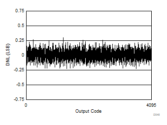
| DNL | Differential non-linearity | TA = 25°C | ±0.25 | LSB | |||
| TA = TMIN to TMAX | ±0.3 | ||||||
| Peak NPR | Peak noise power ratio | 500-kHz tone spacing from 1 MHz to ƒS / 2−1 MHz, DDC bypass mode 25-MHz wide notch at 320 MHz |
46 | dB | |||
| IMD3 | Third-order intermodulation distortion | F1 = 2110 MHz at −13 dBFS F2 = 2170 MHz at −13 dBFS |
–64 | dBc | |||
| DDC BYPASS MODE | |||||||
| SNR1 | Signal-to-noise ratio, integrated across entire Nyquist bandwidth Input frequency-dependent interleaving spurs included |
FIN = 350 MHz, –1 dBFS, 12-bit DDC bypass mode | 55 | dBFS | |||
| FIN = 600 MHz, –1 dBFS, 12-bit DDC bypass mode | TA = 25°C | 54.8 | |||||
| TA = TMIN to TMAX | 52.5 | ||||||
| TA = 25°C, calibration = BG | 53.9 | ||||||
| TA = TMIN to TMAX, calibration = BG | 49.4 | ||||||
| FIN = 1500 MHz, –1 dBFS, 12-bit DDC bypass mode | 51.2 | ||||||
| FIN = 2400 MHz, –1 dBFS, 12-bit DDC bypass mode | 48.7 | ||||||
| SNR2 | Signal-to-noise ratio, integrated across entire Nyquist bandwidth Input frequency-dependent interleaving spurs excluded |
FIN = 600 MHz, –1 dBFS, 12-bit DDC bypass mode | TA = 25°C(4) | 55 | dBFS | ||
| TA = TMIN to TMAX(4) | 53 | ||||||
| TA = 25°C, calibration = BG(4) | 55 | ||||||
| TA = TMIN to TMAX, calibration = BG(4) | 53 | ||||||
| SINAD1 | Signal-to-noise and distortion ratio, integrated across entire Nyquist bandwidth Input frequency-dependent interleaving spurs included |
FIN = 350 MHz, –1 dBFS, 12-bit DDC bypass mode | 54.8 | dBFS | |||
| FIN = 600 MHz, –1 dBFS, 12-bit DDC bypass mode | TA = 25°C | 54.7 | |||||
| TA = TMIN to TMAX | 52.3 | ||||||
| TA = 25°C, calibration = BG | 53.8 | ||||||
| TA = TMIN to TMAX, calibration = BG | 49.2 | ||||||
| FIN = 1500 MHz, –1 dBFS, 12-bit DDC bypass mode | 51.1 | ||||||
| FIN = 2400 MHz, –1 dBFS, 12-bit DDC bypass mode | 48.7 | ||||||
| SINAD2 | Signal-to-noise and distortion ratio, integrated across DDC output bandwidth Input frequency-dependent interleaving spurs excluded |
FIN = 600 MHz, –1 dBFS, 12-bit DDC bypass mode | TA = 25°C(4) | 54.9 | dBFS | ||
| TA = TMIN to TMAX(4) | 52.7 | ||||||
| TA = 25°C, calibration = BG(4) | 54.9 | ||||||
| TA = TMIN to TMAX, calibration = BG(4) | 52.7 | ||||||
| ENOB1 | Effective number of bits, integrated across entire Nyquist bandwidth Input frequency-dependent interleaving spurs included |
FIN = 350 MHz, –1 dBFS, 12-bit DDC bypass mode | 8.8 | Bits | |||
| FIN = 600 MHz, –1 dBFS, 12-bit DDC bypass mode | TA = 25°C | 8.8 | |||||
| TA = TMIN to TMAX | 8.4 | ||||||
| TA = 25°C, calibration = BG | 8.7 | ||||||
| TA = TMIN to TMAX, calibration = BG | 7.9 | ||||||
| FIN = 1500 MHz, –1 dBFS, 12-bit DDC bypass mode | 8.2 | ||||||
| FIN = 2400 MHz, –1 dBFS, 12-bit DDC bypass mode | 7.8 | ||||||
| ENOB2 | Effective number of bits, integrated across entire Nyquist bandwidth Input frequency-dependent interleaving spurs excluded |
FIN = 600 MHz, –1 dBFS, 12-bit DDC bypass mode | TA = 25°C(4) | 8.8 | Bits | ||
| TA = TMIN to TMAX(4) | 8.5 | ||||||
| TA = 25°C, calibration = BG(4) | 8.8 | ||||||
| TA = TMIN to TMAX, calibration = BG(4) | 8.5 | ||||||
| SFDR1 | Spurious-free dynamic range Input frequency-dependent interleaving spurs included |
FIN = 350 MHz, –1 dBFS, 12-bit DDC bypass mode | 67.4 | dBFS | |||
| FIN = 600 MHz, –1 dBFS, 12-bit DDC bypass mode | TA = 25°C | 70.7 | |||||
| TA = TMIN to TMAX | 60 | ||||||
| TA = 25°C, calibration = BG | 63.4 | ||||||
| TA = TMIN to TMAX, calibration = BG | 51.8 | ||||||
| FIN = 1500 MHz, –1 dBFS, 12-bit DDC bypass mode | 59.8 | ||||||
| FIN = 2400 MHz, –1 dBFS, 12-bit DDC bypass mode | 57.2 | ||||||
| SFDR2 | Spurious-free dynamic range Input frequency-dependent interleaving spurs excluded |
FIN = 600 MHz, –1 dBFS, 12-bit DDC bypass mode | TA = 25°C(4) | 73 | dBFS | ||
| TA = TMIN to TMAX(4) | 61.6 | ||||||
| TA = 25°C, calibration = BG(4) | 74 | ||||||
| TA = TMIN to TMAX, calibration = BG (4)mode | 62.8 | ||||||
| ƒS/2 | Interleaving offset spur at ½ sampling rate | FIN = 350 MHz, –1 dBFS, 12-bit DDC bypass mode | –75 | dBFS | |||
| FIN = 600 MHz, –1 dBFS, 12-bit DDC bypass mode | TA = 25°C | –76 | |||||
| TA = TMIN to TMAX | –60 | ||||||
| TA = 25°C, calibration = BG | –68 | ||||||
| TA = TMIN to TMAX, calibration = BG | –55 | ||||||
| FIN = 1500 MHz, –1 dBFS, 12-bit DDC bypass mode | –75 | ||||||
| FIN = 2400 MHz, –1 dBFS, 12-bit DDC bypass mode | –75 | ||||||
| ƒS/4 | Interleaving offset spur at ¼ sampling rate | FIN = 350 MHz, –1 dBFS, 12-bit DDC bypass mode | –68 | dBFS | |||
| FIN = 600 MHz, –1 dBFS, 12-bit DDC bypass mode | TA = 25°C | –70 | |||||
| TA = TMIN to TMAX | –55 | ||||||
| TA = 25°C, calibration = BG | –61 | ||||||
| TA = TMIN to TMAX, calibration = BG | –47.4 | ||||||
| FIN = 1500 MHz, –1 dBFS, 12-bit DDC bypass mode | –68 | ||||||
| FIN = 2400 MHz, –1 dBFS, 12-bit DDC bypass mode | –68 | ||||||
| ƒS/2 – FIN | Interleaving offset spur at ½ sampling rate – input frequency | FIN = 600 MHz, –1 dBFS, 12-bit DDC bypass mode | TA = 25°C | –77 | dBFS | ||
| TA = TMIN to TMAX | –61.7 | ||||||
| TA = 25°C, calibration = BG | –70 | ||||||
| TA = TMIN to TMAX, calibration = BG | –51.9 | ||||||
| ƒS/4 + FIN | Interleaving offset spur at ¼ sampling rate + input frequency | FIN = 600 MHz, –1 dBFS, 12-bit DDC bypass mode | TA = 25°C | –74 | dBFS | ||
| TA = TMIN to TMAX | –60 | ||||||
| TA = 25°C, calibration = BG | –66 | ||||||
| TA = TMIN to TMAX, calibration = BG | –52 | ||||||
| ƒS/4 – FIN | Interleaving offset spur at ¼ sampling rate – input frequency | FIN = 600 MHz, –1 dBFS, 12-bit DDC bypass mode | TA = 25°C | –76 | dBFS | ||
| TA = TMIN to TMAX | –60.4 | ||||||
| TA = 25°C, calibration = BG | –67 | ||||||
| TA = TMIN to TMAX, calibration = BG | –53.3 | ||||||
| THD | Total harmonic distortion | FIN = 350 MHz, –1 dBFS, 12-bit DDC bypass mode | –72 | dBFS | |||
| FIN = 600 MHz, –1 dBFS, 12-bit DDC bypass mode | TA = 25°C | –70 | |||||
| TA = TMIN to TMAX | –60 | ||||||
| TA = 25°C, calibration = BG | –72 | ||||||
| TA = TMIN to TMAX, calibration = BG | –60 | ||||||
| FIN = 1500 MHz, –1 dBFS, 12-bit DDC bypass mode | –68 | ||||||
| FIN = 2400 MHz, –1 dBFS, 12-bit DDC bypass mode | –74 | ||||||
| HD2 | Second harmonic distortion | FIN = 350 MHz, –1 dBFS, 12-bit DDC bypass mode | –85 | dBFS | |||
| FIN = 600 MHz, –1 dBFS, 12-bit DDC bypass mode | TA = 25°C | –80 | |||||
| TA = TMIN to TMAX | –62 | ||||||
| TA = 25°C, calibration = BG | –80 | ||||||
| TA = TMIN to TMAX, calibration = BG | –62.5 | ||||||
| FIN = 1500 MHz, –1 dBFS, 12-bit DDC bypass mode | –71 | ||||||
| FIN = 2400 MHz, –1 dBFS, 12-bit DDC bypass mode | –79 | ||||||
| HD3 | Third harmonic distortion | FIN = 350 MHz, –1 dBFS, 12-bit DDC bypass mode | –73 | dBFS | |||
| FIN = 600 MHz, –1 dBFS, 12-bit DDC bypass mode | TA = 25°C | –75 | |||||
| TA = TMIN to TMAX | –61 | ||||||
| TA = 25°C, calibration = BG | –80 | ||||||
| TA = TMIN to TMAX, calibration = BG | –61.7 | ||||||
| FIN = 1500 MHz, –1 dBFS, 12-bit DDC bypass mode | –74 | ||||||
| FIN = 2400 MHz, –1 dBFS, 12-bit DDC bypass mode | –76 | ||||||
| NSD | Noise spectral density, average NSD across Nyquist bandwidth | 12-bit DDC bypass mode | 50-Ω AC-coupled terminated input | –149 | dBFS/Hz | ||
| –150.8 | dBm/Hz | ||||||
| FIN = 600 MHz, –1 dBFS | –147.8 | dBFS/Hz | |||||
| –149.6 | dBm/Hz | ||||||
| DECIMATE-BY-8 MODE | |||||||
| SNR1 | Signal-to-noise ratio, integrated across DDC output bandwidth Interleaving spurs included |
FIN = 600 MHz, –1 dBFS, decimate-by-8 mode | 63 | dBFS | |||
| Calibration = BG | 61.6 | ||||||
| FIN = 2400 MHz, –1 dBFS, decimate-by-8 mode | 54.6 | ||||||
| SNR2 | Signal-to-noise ratio, integrated across DDC output bandwidth Interleaving spurs excluded |
FIN = 600 MHz, –1 dBFS, decimate-by-8 mode(4) | 63.3 | dBFS | |||
| Calibration = BG | 63.3 | ||||||
| SINAD1 | Signal-to-noise and distortion ratio, integrated across DDC output bandwidth Interleaving spurs included |
FIN = 600 MHz, –1 dBFS, Decimate-by-8 mode | 63 | dBFS | |||
| Calibration = BG | 61.6 | ||||||
| FIN = 2400 MHz, –1 dBFS, decimate-by-8 mode | 54.6 | ||||||
| SINAD2 | Signal-to-noise and distortion ratio, integrated across DDC output bandwidth Interleaving spurs excluded |
FIN = 600 MHz, –1 dBFS, decimate-by-8 mode(4) | 63.3 | dBFS | |||
| Calibration = BG | 63.3 | ||||||
| ENOB1 | Effective number of bits, integrated across DDC output bandwidth Interleaving spurs included |
FIN = 600 MHz, –1 dBFS, decimate-by-8 mode | 10.2 | Bits | |||
| Calibration = BG | 10.0 | ||||||
| FIN = 2400 MHz, –1 dBFS, decimate-by-8 mode | 8.8 | ||||||
| ENOB2 | Effective number of bits, integrated across DDC output bandwidth Interleaving spurs excluded |
FIN = 600 MHz, –1 dBFS, decimate-by-8 mode(5) | 10.2 | Bits | |||
| Calibration = BG | 10.2 | ||||||
| SFDR1 | Spurious-free dynamic range Interleaving Spurs Included |
FIN = 600 MHz, –1 dBFS, decimate-by-8 mode | 74.9 | dBFS | |||
| Calibration = BG | 68.3 | ||||||
| SFDR2 | Spurious-free dynamic range Interleaving spurs excluded |
FIN = 600 MHz, –1 dBFS, decimate-by-8 mode(5) | 77.8 | dBFS | |||
| Calibration = BG | 77.8 | ||||||
| ƒS/2 | Interleaving offset spur at ½ sampling rate(5) | FIN = 600 MHz, –1 dBFS, decimate-by-8 mode | –73 | dBFS | |||
| Calibration = BG | –72 | ||||||
| ƒS/4 | Interleaving offset spur at ¼ sampling rate(5) | FIN = 600 MHz, –1 dBFS, decimate-by-8 mode | –70 | dBFS | |||
| Calibration = BG | –66 | ||||||
| ƒS/2 – FIN | Interleaving spur at ½ sampling rate – input frequency(5) | FIN = 600 MHz, –1 dBFS, decimate-by-8 mode | –76 | dBFS | |||
| Calibration = BG | –67 | ||||||
| ƒS/4 + FIN | Interleaving spur at ¼ sampling rate + input frequency(5) | FIN = 600 MHz, –1 dBFS, decimate-by-8 mode | –72 | dBFS | |||
| Calibration = BG | –64 | ||||||
| ƒS/4 – FIN | Interleaving spur at ¼ sampling rate – input frequency(5) | FIN = 600 MHz, –1 dBFS, decimate-by-8 mode | –74 | dBFS | |||
| Calibration = BG | –67 | ||||||
| THD | Total harmonic distortion(6) | FIN = 600 MHz, –1 dBFS, decimate-by-8 mode | –70 | dBFS | |||
| Calibration = BG | –72 | ||||||
| FIN = 2400 MHz, –1 dBFS, decimate-by-8 mode | –71 | ||||||
| HD2 | Second harmonic distortion(6) | FIN = 600 MHz, –1 dBFS, decimate-by-8 mode | –80 | dBFS | |||
| Calibration = BG | –79 | ||||||
| FIN = 2400 MHz, –1 dBFS, decimate-by-8 mode | –78 | ||||||
| HD3 | Third harmonic distortion(6) | FIN = 600 MHz, –1 dBFS, decimate-by-8 mode | –74 | dBFS | |||
| Calibration = BG | –80 | ||||||
| FIN = 2400 MHz, –1 dBFS, decimate-by-8 mode | –-77 | ||||||
| DDC CHARACTERISTICS | |||||||
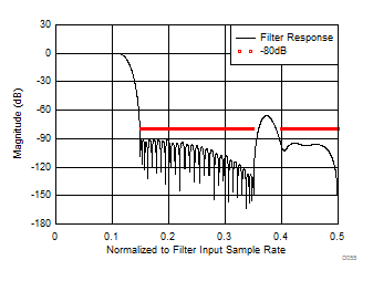
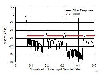
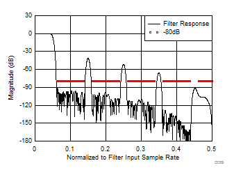
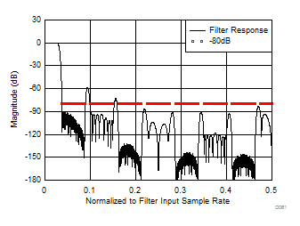
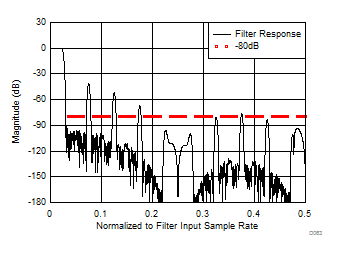
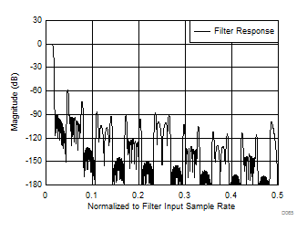
| Alias protection(2) | 80 | dB | |||||
| Alias protected bandwidth(2) | 80 | % of output BW | |||||
| SFDR-DDC | Spurious-free dynamic range of digital down-converter(2) | 100 | dB | ||||
| Implementation loss(2) | 0.5 | dB | |||||
| ANALOG INPUT CHARACTERISTICS | |||||||
| VID(VIN) | Full-scale analog-differential input range | Minimum FSR setting(6) | 500 | mVPP | |||
| Default FSR setting, TA = TMIN to TMAX | 650 | 725 | 800 | ||||
| Maximum FSR setting(6) | 950 | ||||||
| CI(VIN) | Analog input capacitance(2) | Differential | 0.05 | pF | |||
| Each input pin to ground | 1.5 | pF | |||||
| RID(VIN) | Differential input resistance | 80 | 95 | 110 | Ω | ||
| FPBW | Full power bandwidth | –3 dB — calibration = BG | 2.8 | GHz | |||
| –3 dB — calibration = FG | 3.2 | ||||||
| Gain flatness | DC to 2 GHz | 1.2 | dB | ||||
| 2 GHz to 4 GHz | 3.8 | ||||||
| DC to 2 GHz — calibration = BG | 1.5 | ||||||
| 2 GHz to 4 GHz — calibration = BG | 4.5 | ||||||
| ANALOG OUTPUT CHARACTERISTICS (VCMO, VBG) | |||||||
| V(VCMO) | Common-mode output voltage | I(VCMO) = ±100 µA, TA = 25°C | 1.225 | V | |||
| I(VCMO) = ±100 µA, TA = TMIN to TMAX | 1.185 | 1.265 | |||||
| TCVO(VCMO) | Common-mode output-voltage temperature coefficient | TA = TMIN to TMAX | -21 | ppm/°C | |||
| C(LOAD_VCMO) | Maximum VCMO output load capacitance | 80 | pF | ||||
| VO(BG) | Bandgap reference output voltage | I(BG) = ±100 µA, TA = 25°C | 1.248 | V | |||
| I(BG) = ±100 µA, TA = TMIN to TMAX | 1.195 | 1.3 | |||||
| TCVref(BG) | Bandgap reference voltage temperature coefficient | TA = TMIN to TMAX, I(BG) = ±100 µA |
0 | ppm/°C | |||
| C(LOAD_BG) | Maximum bandgap reference output load capacitance | 80 | pF | ||||
| TEMPERATURE DIODE CHARACTERISTICS | |||||||
| V(TDIODE) | Temperature diode voltage slope | Offset voltage (approx. 0.77 V) varies with process and must be measured for each part. Offset measurement should be done with PowerDown=1 to minimize device self-heating. | 100-µA forward current Device active |
–1.6 | mV/°C | ||
| 100-µA forward current Device in power-down |
–1.6 | mV/°C | |||||
| CLOCK INPUT CHARACTERISTICS (DEVCLK±, SYSREF±, SYNC~/TMST±) | |||||||
| VID(CLK) | Differential clock input level | Sine wave clock, TA = TMIN to TMAX | 0.4 | 0.6 | 2 | VPP | |
| Square wave clock, TA = TMIN to TMAX | 0.4 | 0.6 | 2 | VPP | |||
| II(CLK) | Input current | VI = 0 or VI = VA | ±1 | µA | |||
| CI(CLK) | Input capacitance(2) | Differential | 0.02 | pF | |||
| Each input to ground | 1 | pF | |||||
| RID(CLK) | Differential input resistance | TA = 25°C | 95 | Ω | |||
| TA = TMIN to TMAX | 80 | 110 | Ω | ||||
| CML OUTPUT CHARACTERISTICS (DS0–DS7±) | |||||||
| VOD | Differential output voltage | Assumes ideal 100-Ω load Measured differentially Default pre-emphasis setting |
280 | 305 | 330 | mV peak | |
| VO(ofs) | Output offset voltage | 0.6 | V | ||||
| IOS | Output short-circuit current | Output+ and output– shorted together | ±6 | mA | |||
| Output+ or output– shorted to 0 V | 12 | ||||||
| ZOD | Differential output impedance | 100 | Ω | ||||
| LVCMOS INPUT CHARACTERISTICS (SDI, SCLK, SCS, SYNC~) | |||||||
| VIH | Logic high input voltage | See (6) | 0.83 | V | |||
| VIL | Logic low input voltage | See (6) | 0.4 | V | |||
| CI | Input capacitance(2)(7) | Each input to ground | 1 | pF | |||
| LVCMOS OUTPUT CHARACTERISTICS (SDO, OR_T0, OR_T1) | |||||||
| VOH | CMOS H level output | IOH = –400 µA(6) | 1.65 | 1.9 | V | ||
| VOL | CMOS L level output | IOH = 400 µA(6) | 0.01 | 0.15 | V | ||
| POWER SUPPLY CHARACTERISTICS | |||||||
| I(VA19) | Analog 1.9-V supply current | PD = 0, calibration = FG, bypass DDC | 461 | 500 | mA | ||
| PD = 0, calibration = BG, bypass DDC | 560 | 600 | |||||
| PD = 0, calibration = BG, decimate by 8, DDR = 0, P54 = 1 | 560 | 607 | |||||
| I(VA12) | Analog 1.2-V supply current | PD = 0, calibration = FG, bypass DDC | 320 | 385 | mA | ||
| PD = 0, calibration = BG, bypass DDC | 364 | 420 | |||||
| PD = 0, calibration = BG, decimate by 8, DDR = 0, P54 = 1 | 377 | 428 | |||||
| I(VD12) | Digital 1.2-V supply current | PD = 0, calibration = FG, bypass DDC | 445 | 710 | mA | ||
| PD = 0, calibration = BG, bypass DDC | 458 | 732 | |||||
| PD = 0, calibration = BG, decimate by 8, DDR = 0, P54 = 1 | 541 | 826 | |||||
| PC | Power consumption | PD = 0, calibration = FG, bypass DDC | 1.8 | 2.26 | W | ||
| PD = 0, calibration = BG, bypass DDC | 2.05 | 2.52 | |||||
| PD = 0, calibration = BG, decimate by 8, DDR = 0, P54 = 1 | 2.17 | 2.66 | |||||
| PD = 1 | < 50 | mW | |||||
(1) To ensure accuracy, the VA19, VA12, and VD12 pins are required to be well bypassed. Each supply pin must be decoupled with one or more bypass capacitors.
(2) This parameter is specified by design and is not tested in production.
(3) Interleave related fixed frequency spurs at ƒS / 4 and ƒS / 2 are excluded from all SNR, SINAD, ENOB and SFDR specifications. The magnitude of these spurs is provided separately.
(4) Interleave related spurs at ƒS / 2 – FIN, ƒS / 4 + FIN and ƒS / 4 – FIN are excluded from these performance calculations. The magnitude of these spurs is provided separately.
(5) Magnitude of reported tones in output spectrum of ADC core. This tone will only be present in the DDC output for specific Decimation and NCO settings. Careful frequency planning can be used to intentionally place unwanted tones outside the DDC output spectrum.
(6) This parameter is specified by design, characterization, or both and is not tested in production.
(7) The digital control pin capacitances are die capacitances only and is in addition to package and bond-wire capacitance of approximately 0.4 pF.
6.6 Timing Requirements
| MIN | NOM | MAX | UNIT | |||
|---|---|---|---|---|---|---|
| DEVICE (SAMPLING) CLOCK | ||||||
| ƒ(DEVCLK) | Input DEVCLK frequency | Sampling rate is equal to clock input | 1 | 4 | GHz | |
| td(A) | Sampling (aperture) delay | Input CLK transition to sampling instant | 0.64 | ns | ||
| t(AJ) | Aperture jitter | 0.1 | ps RMS | |||
| t(LAT) | ADC core latency(2) | Decimation = 1, DDR = 1, P54 = 0 | 64 | t(DEVCLK) | ||
| t(LAT_DDC) | ADC core and DDC latency(2) | Decimation = 4, DDR = 1, P54 = 0 | 292 | t(DEVCLK) | ||
| Decimation = 4, DDR = 1, P54 = 1 | 284 | |||||
| Decimation = 8, DDR = 0, P54 = 0 | 384 | |||||
| Decimation = 8, DDR = 0, P54 = 1 | 368 | |||||
| Decimation = 8, DDR = 1, P54 = 0 | 392 | |||||
| Decimation = 8, DDR = 1, P54 = 1 | 368 | |||||
| Decimation = 10, DDR = 0, P54 = 0 | 386 | |||||
| Decimation = 10, DDR = 1, P54 = 0 | 386 | |||||
| Decimation = 16, DDR = 0, P54 = 0 | 608 | |||||
| Decimation = 16, DDR = 0, P54 = 1 | 560 | |||||
| Decimation = 16, DDR = 1, P54 = 0 | 608 | |||||
| Decimation = 16, DDR = 1, P54 = 1 | 560 | |||||
| Decimation = 20, DDR = 0, P54 = 0 | 568 | |||||
| Decimation = 20, DDR = 1, P54 = 0 | 568 | |||||
| Decimation = 32, DDR = 0, P54 = 0 | 1044 | |||||
| Decimation = 32, DDR = 0, P54 = 1 | 948 | |||||
| Decimation = 32, DDR = 1, P54 = 0 | 1044 | |||||
| JESD204B INTERFACE LINK TIMING CHARACTERISTICS (REFER TO Figure 1) | ||||||
| td(LMFC) | SYSREF to LMFC delay Functional delay between SYSREF assertion latched and LMFC frame boundary(2) |
All decimation modes | 40 | t(DEVCLK) | ||
| td(TX) | LMFC to frame boundary delay - DDC bypass mode Functional delay from LMFC frame boundary to beginning of next multi-frame in transmitted data.(3) |
Decimation = 1, DDR = 1, P54 = 0 | 52.7 | t(DEVCLK) | ||
| td(TX) | LMFC to frame boundary delay - decimation modes Functional delay from LMFC frame boundary to beginning of next multi-frame in transmitted data(3) |
Decimation = 4, DDR = 1, P54 = 0 | 52.7 | t(DEVCLK) | ||
| Decimation = 4, DDR = 1, P54 = 1 | 43.9 | |||||
| Decimation = 8, DDR = 0, P54 = 0 | 60.7 | |||||
| Decimation = 8, DDR = 0, P54 = 1 | 51.5 | |||||
| Decimation = 8, DDR = 1, P54 = 0 | 52.7 | |||||
| Decimation = 8, DDR = 1, P54 = 1 | 43.9 | |||||
| Decimation = 10, DDR = 0, P54 = 0 | 60.7 | |||||
| Decimation = 10, DDR = 1, P54 = 0 | 52.7 | |||||
| Decimation = 16, DDR = 0, P54 = 0 | 60.7 | |||||
| Decimation = 16, DDR = 0, P54 = 1 | 51.5 | |||||
| Decimation = 16, DDR = 1, P54 = 0 | 52.7 | |||||
| Decimation = 16, DDR = 1, P54 = 1 | 43.9 | |||||
| Decimation = 20, DDR = 0, P54 = 0 | 60.7 | |||||
| Decimation = 20, DDR = 1, P54 = 0 | 52.7 | |||||
| Decimation = 32, DDR = 0, P54 = 0 | 60.7 | |||||
| Decimation = 32, DDR = 0, P54 = 1 | 51.5 | |||||
| Decimation = 32, DDR = 1, P54 = 0 | 52.7 | |||||
| tsu(SYNC~-F) | SYNC~ to LMFC setup time(1)
Required SYNC~ setup time relative to the internal LMFC boundary. |
40 | t(DEVCLK) | |||
| th(SYNC~-F) | SYNC~ to LMFC hold time(1)
Required SYNC~ hold time relative to the internal LMFC boundary. |
–8 | ||||
| t(SYNC~) | SYNC~ assertion time Required SYNC~ assertion time before deassertion to initiate a link resynchronization. |
4 | Frame clock cycles | |||
| td(LMFC) | Delay from SYSREF sampled high by DEVCLK to internal LMFC boundary | 40 | t(DEVCLK) | |||
| t(ILA) | Duration of initial lane alignment sequence | 4 | Multi-frame clock cycles | |||
| SYSREF | ||||||
| tsu(SYS) | Setup time SYSREF relative to DEVCLK rising edge(6) | 40 | ps | |||
| th(SYS) | Hold time SYSREF relative to DEVCLK rising edge(6) | 40 | ps | |||
| t(PH_SYS) | SYSREF assertion duration after rising edge event. | 8 | t(DEVCLK) | |||
| t(PL_SYS) | SYSREF deassertion duration after falling edge event. | 8 | t(DEVCLK) | |||
| t(SYS) | Period SYSREF± | DDR = 0, P54 = 0 | K × F × 10 | t(DEVCLK) | ||
| DDR = 0, P54 = 1 | K × F × 8 | |||||
| DDR = 1, P54 = 0 | K × F × 5 | |||||
| DDR = 1, P54 = 1 | K × F × 4 | |||||
| SERIAL INTERFACE (REFER TO Figure 2) | ||||||
| ƒ(SCK) | Serial clock frequency(2) | 20 | MHz | |||
| t(PH) | Serial clock high time | 20 | ns | |||
| t(PL) | Serial clock low time | 20 | ns | |||
| tsu | Serial-data to serial-clock rising setup time(2) | 10 | ns | |||
| th | Serial-data to serial clock rising hold time(2) | 10 | ns | |||
| t(CSS) | SCS-to-serial clock rising setup time | 10 | ns | |||
| t(CSH) | SCS-to-serial clock falling hold time | 10 | ns | |||
| t(IAG) | Inter-access gap | 10 | ns | |||
(1) This parameter must be met to achieve deterministic alignment of the data frame and NCO phase to other similar devices. If this parameter is not met the device will still function correctly but will not be aligned to other devices.
(2) Unless otherwise specified, delays quoted are exact un-rounded functional delays (assuming zero propagation delay).
(3) The values given are functional delays only. Additional propagation delay of 0 to 3 clock cycles will be present.
6.7 Internal Characteristics
| PARAMETER | TEST CONDITIONS | MIN | NOM | MAX | UNIT | |
|---|---|---|---|---|---|---|
| DEVICE (SAMPLING) CLOCK | ||||||
| td(A) | Sampling (aperture) delay | Input CLK transition to sampling instant | 0.64 | ns | ||
| t(AJ) | Aperture jitter | 0.1 | ps RMS | |||
| t(LAT) | ADC core latency. See (2) | Decimation = 1, DDR = 1, P54 = 0 | 64 | t(DEVCLK) | ||
| CALIBRATION TIMING CHARACTERISTICS (REFER TO THE CALIBRATION SECTION) | ||||||
| t(CAL) | Calibration cycle time | Calibration = FG, T_AUTO=1 | 227 × 106 | t(DEVCLK) | ||
| Calibration = FG, T_AUTO=0 | 102 × 106 | |||||
| JESD204B INTERFACE LINK TIMING CHARACTERISTICS (REFER TO Figure 1) | ||||||
| td(LMFC) | SYSREF to LMFC delay Functional delay between SYSREF assertion latched and LMFC frame boundary(2) |
All decimation modes | 40 | t(DEVCLK) | ||
| td(TX) | LMFC to Frame Boundary delay - DDC Bypass Mode Functional delay from LMFC frame boundary to beginning of next multi-frame in transmitted data(3) |
Decimation = 1, DDR = 1, P54 = 0 | 52.7 | t(DEVCLK) | ||
| td(TX) | LMFC to frame boundary delay - decimation modes Functional delay from LMFC frame boundary to beginning of next multi-frame in transmitted data(3) |
Decimation = 4, DDR = 1, P54 = 0 | 52.7 | t(DEVCLK) | ||
| Decimation = 4, DDR = 1, P54 = 1 | 43.9 | |||||
| Decimation = 8, DDR = 0, P54 = 0 | 60.7 | |||||
| Decimation = 8, DDR = 0, P54 = 1 | 51.5 | |||||
| Decimation = 8, DDR = 1, P54 = 0 | 52.7 | |||||
| Decimation = 8, DDR = 1, P54 = 1 | 43.9 | |||||
| Decimation = 10, DDR = 0, P54 = 0 | 60.7 | |||||
| Decimation = 10, DDR = 1, P54 = 0 | 52.7 | |||||
| Decimation = 16, DDR = 0, P54 = 0 | 60.7 | |||||
| Decimation = 16, DDR = 0, P54 = 1 | 51.5 | |||||
| Decimation = 16, DDR = 1, P54 = 0 | 52.7 | |||||
| Decimation = 16, DDR = 1, P54 = 1 | 43.9 | |||||
| Decimation = 20, DDR = 0, P54 = 0 | 60.7 | |||||
| Decimation = 20, DDR = 1, P54 = 0 | 52.7 | |||||
| Decimation = 32, DDR = 0, P54 = 0 | 60.7 | |||||
| Decimation = 32, DDR = 0, P54 = 1 | 51.5 | |||||
| Decimation = 32, DDR = 1, P54 = 0 | 52.7 | |||||
| td(LMFC) | Delay from SYSREF sampled high by DEVCLK to internal LMFC boundary | 40 | t(DEVCLK) | |||
| t(ILA) | Duration of initial lane alignment sequence | 4 | Multi-frame clock cycles | |||
6.8 Switching Characteristics
Unless otherwise noted, these specifications apply for V(VA12) = V(VD12) = 1.2 V, V(VA19) = 1.9 V, VIN FSR (AC coupled) = Default setting, differential AC-coupled sinewave input clock, ƒ(DEVCLK) = 4 GHz at 0.5 VPP with 50% duty cycle, R(RBIAS) = 3.3 kΩ ±0.1%, after a foreground mode calibration with timing calibration enabled. Typical values are at TA = 25°C.| PARAMETER | TEST CONDITIONS | MIN | TYP | MAX | UNIT | |
|---|---|---|---|---|---|---|
| SERIAL DATA OUTPUTS | ||||||
| Serialized output bit rate | 1 | 10 | Gbps | |||
| Serialized output bit rate | DDR = 0, P54 = 0 | ƒS | ||||
| DDR = 0, P54 = 1 | 1.25 × ƒS | |||||
| DDR = 1, P54 = 0 | 2 × ƒS | |||||
| DDR = 1, P54 = 1 | 2.5 × ƒS | |||||
| tTLH | LH transition time — differential | 10% to 90%, 8 Gbps | 35 | ps | ||
| tTHL | HL transition time — differential | 10% to 90%, 8 Gbps | 35 | ps | ||
| UI | Unit interval | 8 Gbps serial rate | 125 | ps | ||
| DDJ | Data dependent jitter | 8 Gbps serial rate | 11.3 | ps | ||
| RJ | Random Jitter | 8 Gbps serial rate | 1.4 | ps | ||
| SERIAL INTERFACE | ||||||
| t(OZD) | SDO tri-state to driven | See Figure 2 | 5 | ns | ||
| t(ODZ) | SDO driven to tri-state | 2.5 | 5 | ns | ||
| t(OD) | SDO output delay | 20 | ns | |||
 Figure 1. JESD204 Synchronization
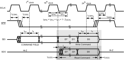 Figure 2. Serial Interface Timing
6.9 Typical Characteristics
Unless otherwise noted, these specifications apply for V(VA12) = V(VD12) = 1.2 V, V(VA19) = 1.9 V, VIN FSR (AC coupled) = Default setting, differential AC-coupled sinewave input clock, ƒ(DEVCLK) = 4 GHz at 0.5 VPP with 50% duty cycle, R(RBIAS) = 3.3 kΩ ±0.1%, after a Foreground mode calibration with Timing Calibration enabled. TA = 25°C. VI = –1 dBFS.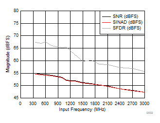
| DDC bypass mode | Sampling rate = 4000 MSPS |
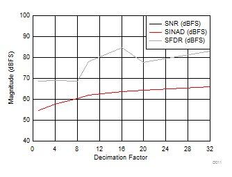
| DDC bypass mode | FIN = 608 MHz |

| DDC bypass mode | FIN = 608 MHz |
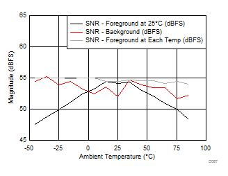
| DDC bypass mode | FIN = 351 MHz |
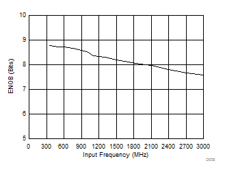
| DDC bypass mode | Sampling rate = 4000 MSPS | ||
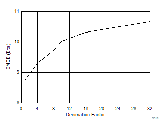
| FIN = 608 MHz |
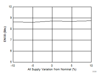
| DDC bypass mode | FIN = 608 MHz |
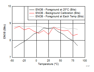
| DDC bypass mode | FIN = 351 MHz |
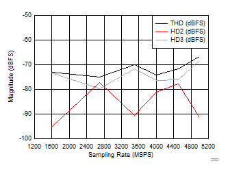
| DDC bypass mode | FIN = 608 MHz | ||
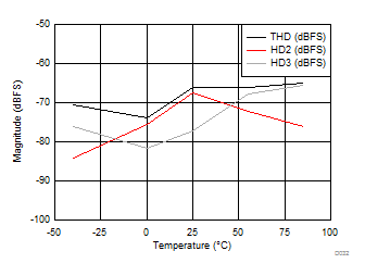
| DDC bypass mode | FIN = 608 MHz |

| DDC bypass mode | FIN = 351 MHz |
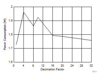
| FIN = 608 MHz |
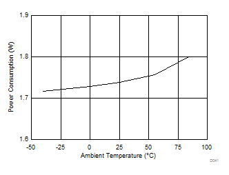
| DDC bypass mode |

| Foreground calibration mode |
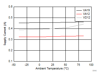
A.
Figure 31. Supply Current vs Temperature
| DDC bypass mode | Foreground calibration mode |
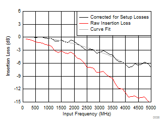
| Background calibration mode |
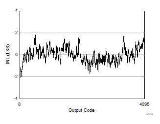
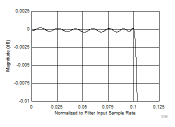
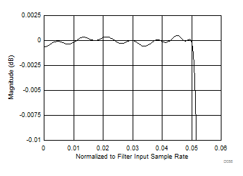
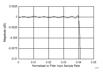
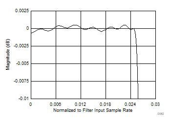
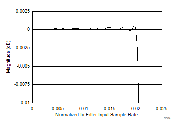

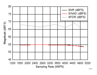
| DDC bypass mode | FIN = 608 MHz |
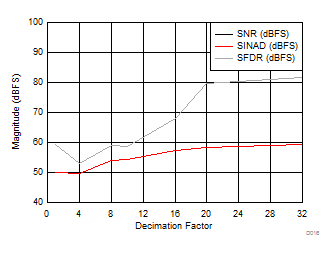
| DDC bypass mode | FIN = 2483 MHz |
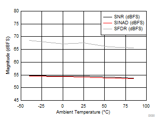
| DDC bypass mode | FIN = 608 MHz |
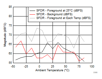
| DDC bypass mode | Input frequency = 351 MHz |
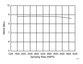
| DDC bypass mode | FIN = 608 MHz | ||
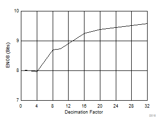
| FIN = 2483 MHz |
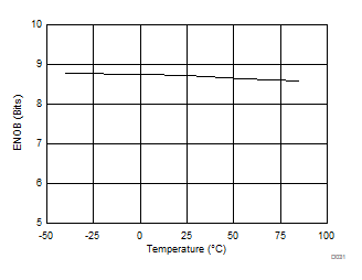
| DDC bypass mode | FIN = 608 MHz |

| DDC bypass mode | Sampling rate = 4000 MSPS | ||
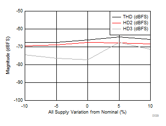
| DDC bypass mode | FIN = 608 MHz |
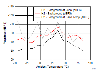
| DDC bypass mode | FIN = 351 MHz |
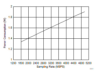
| DDC bypass mode | FIN = 600 MHz | ||
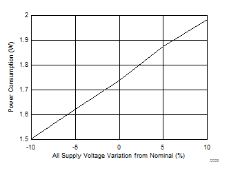
| DDC bypass mode |
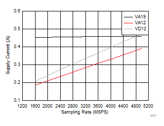
| DDC bypass mode | FIN = 608 MHz | ||
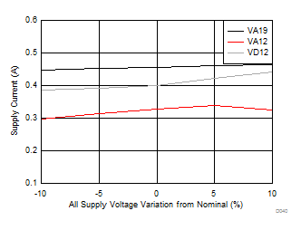
| DDC bypass mode | Foreground calibration mode |
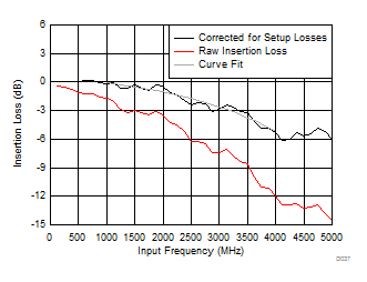
| Foreground calibration mode |
