SLAU833A May 2020 – October 2020
6 Hardware Setup
This section provides directions and illustrations for setting up the hardware.
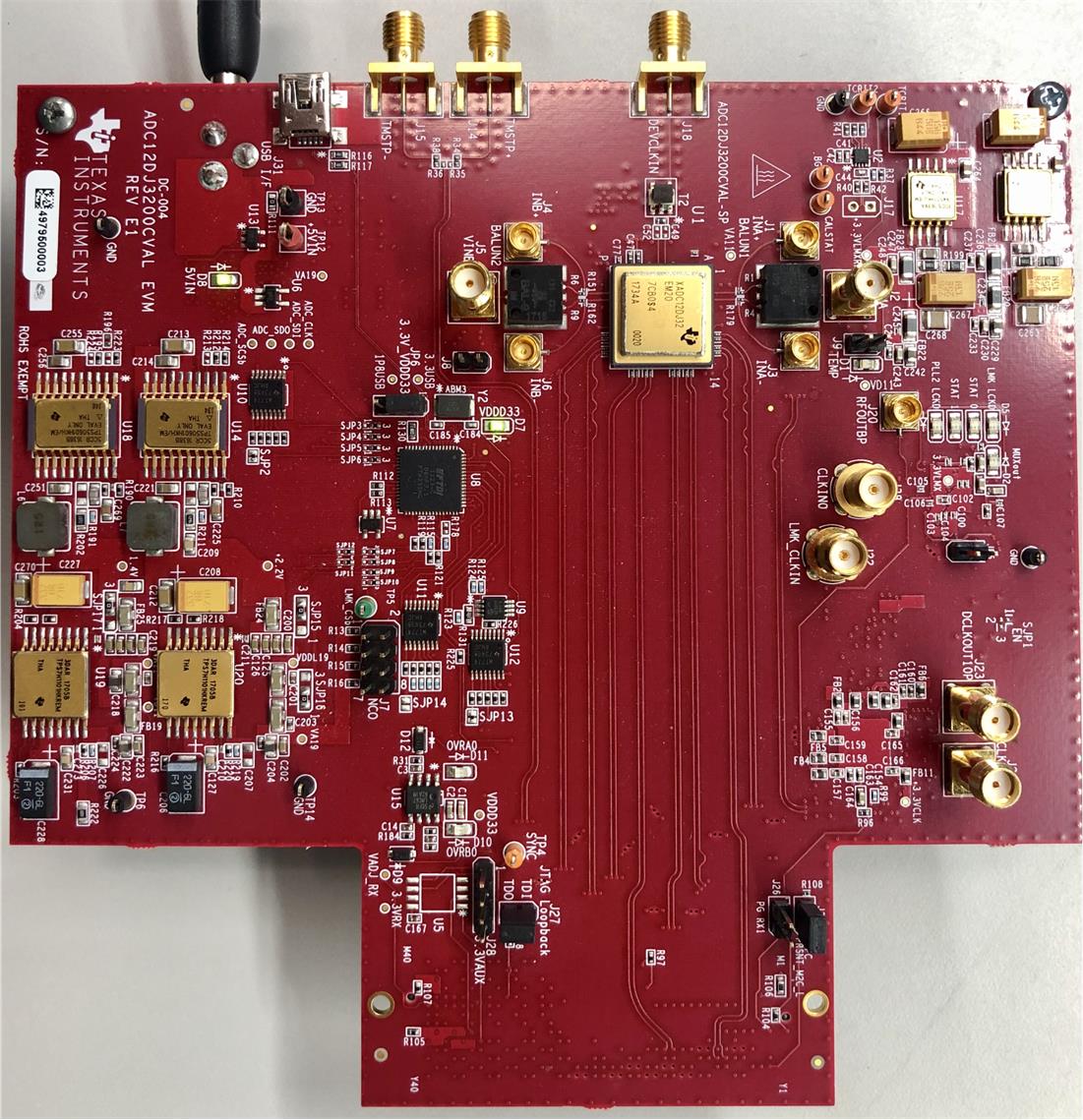 Figure 6-1 ADC12DJ3200EVM Board
By default, the FMC+ interface EEPROM on the ADC12DJ3200EVM is installed. Without this part, the FMC3_VADJ voltage for the FPGA bank that drives the JESD204B SYNC will be set to 0 V, thus preventing the SYNC signal from working. Using the ADC manual SYNC is a work around for this. U5 (24C65T-I/SM from Microchip) is programmed with the provided .bin file called "FMC-ADC12DJ3200-CVAL.bin". This .bin file uses address 0x53 which is required for the FMC+ slot on the Alpha Data board and will set the FMC3_VADJ to 1.8 V after power up. With the EEPROM installed and programmed properly, after power up, test point TP3 on the Alpha Data board should be at 1.8 V.
- Connect the Alpha Data board with ADC12DJ3200 CVAL EVM. Use the FMC+ connector (J3) to connect the ADC EVM.
- Connect the output power cable from the CX 650 power supply to the Alpha Data board as Figure 6-2 shows:
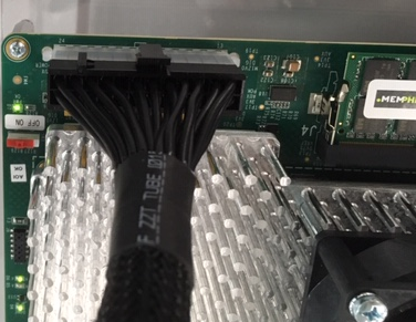 Figure 6-2 Output Power Cable Connection
 - Connect the JTAG cable between the PC and the JTAG port on the USB daughter board.
- Connect a USB cable between USB daughter board and the PC, see Figure 6-3.
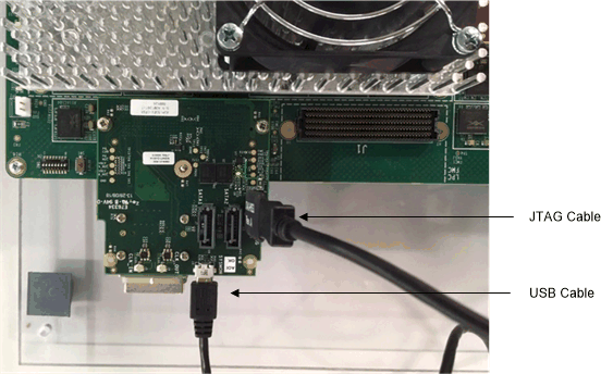 Figure 6-3 JTAG and USB Cable Connections
 - Connect a USB cable between the ADC12DJ3200EVM (J31) and the PC. Connect the 5-V power supply that can source a minimum of 3 A to J37 on the ADC12DJ3200EVM. TP12 (+5 V) and TP13 (GND) provide another option for connecting to 5 V.
- Connect a RF analog input source to J2 (VINA) of the ADC12DJ3200EVM. This guide uses a 70-MHz source at 0 dBm from a TI TSW2700EVM.
- Turn on the Alpha Data board. The power switch is near the power input cable.
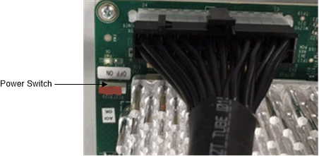 Figure 6-4 Alpha Data Board Power Switch
 - Figure 6-5 illustrates the setup.
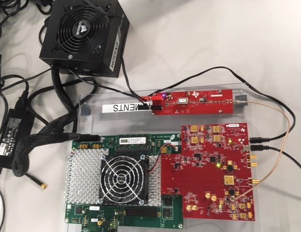 Figure 6-5 Alpha Data Board With ADC12DJ3200 CVAL EVM Setup