SLDU019B December 2015 – March 2016 PGA450-Q1
2.2.3 Testing the UART Connection With the TI GER Board
Use the steps that follow to test the UART connection with the TI GER board.
- If the user has not disconnected the system power, ensure that the MCU is activated again by clicking the ON (MicroActive) on the ESFR tab.
- In the top-right of the PGA450Q1EVM GUI, click the Direct TI GER Control button. This button does not contain text; it is just an image (see the red circle in Figure 4).
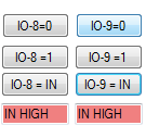
- Under the GPIO tab, clicking the IO-8 = IN and IO-9 = IN buttons to ensure that IO-8 and IO-9 are set as IN HIGH (see Figure 5).
- Connect the UART pins of the sensor to the UART pins of the TI GER board (see Figure 3)
- Pin 10 (TxD) on the TI GER board goes to RXD on the Sensor.
- Pin 20 (RxD) on the TI GER board goes to TXD on the Sensor.
- On the UART tab, under the UART CONTROL SETTING section, select SETUP #9.
- In the BAUD RATE box in the lower right corner of the GUI, enter 19200.
- On the UART TEST tab, Select SETUP #9
- Click the OPEN UART MODULE button.
- Click the CHANGE BAUD RATE button, which should display 19200 and 1-bit = 52.1 μs.
- Click the CHECK FOR ERRORS to ensure there no errors occurred. If an error occurred, one of the boxes will be red, at which point the user must click the CLOSE MODULE IMMEDIATELY and CLOSE UART MODULE buttons. Then repeat the setup, beginning at Step 8 in Section 2.2.3.
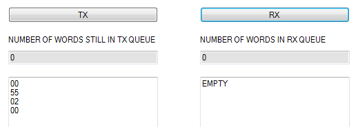
- Write the values shown in Figure 6 in the TX box. Each byte must be typed on a separate row.
- 00: is the break field
- 55: is the synchronization field
- 01: 0 is the command and 1 is the sensor address. Ensure that the sensor address matches what was programmed in the EEPROM address 0x07 from the previous steps.
- 00: is the checksum field; however, this data is discarded, so the user may enter any value here.
- Click the RX button to display the response of the sensor.
- 12: is dummy byte 1 and has no special meaning.
- 34: is dummy byte 2 and has no special meaning.
- B9: is the checksum from byte 1 and byte 2.
 Figure 4. Direct TI GER Control Button
  Figure 5. GPIO Tab
  Figure 6. User Submitted Data Packet in TX Box and Valid RX Response
 The description of the TX data packet is as follows:
The description of the RX data packet is as follows:
The function that calculates the checksum is described as follows:
Table 4 provides a checksum calculation of four bytes shown. If the frame has four data bytes of the protected identifier and three data bytes, the calculation is the same. The data = 0x4A, 0x55, 0x93, 0xE5.
Table 4. Example of Checksum Calculation
| Action | Hex | Carry | D7 | D6 | D5 | D4 | D3 | D2 | D1 | D0 |
|---|---|---|---|---|---|---|---|---|---|---|
| 0x4A | 0x4A | 0 | 1 | 0 | 0 | 1 | 0 | 1 | 0 | |
| +0x55 = Add Carry | 0x9F
0x9F |
0 | 1
1 |
0
0 |
0
0 |
1
1 |
1
1 |
1
1 |
1
1 |
1
1 |
| +0x93 = Add Carry | 0x132
0x33 |
1 | 0
0 |
0
0 |
1
1 |
1
1 |
0
0 |
0
0 |
1
1 |
0
1 |
| +0xE5 = Add Carry | 0x118
0x19 |
1 | 0
0 |
0
0 |
0
0 |
1
1 |
1
1 |
0
0 |
0
0 |
0
1 |
| Invert | 0xE6 | 1 | 1 | 1 | 0 | 0 | 1 | 1 | 0 | |
| 0x19 + 0.xE6 = | 0xFF | 1 | 1 | 1 | 1 | 1 | 1 | 1 | 1 |
The resulting sum is 0x19. Inversion yields the final result of: checksum = 0xE6. The receiving node can check the consistency of the received frame by using the same addition mechanism. When the received checksum (0xE6) is added to the intermediate result (0x19) the sum is 0xFF.
The previously described TX command is called command0 – Sensor Check Command. If the sensor is address 0x01 and the user attempts to communicate with a sensor using a different address, sensor 0x01 gives no response. In the following TX example shown in Figure 7, no response was received as displayed in the RX box because, in this example, command0 was sent to sensor address 0x02.
 Figure 7. No Response in the RX Box